3D Printed Auxetic Structure-Assisted Piezoelectric Energy Harvesting and Sensing
Xinran Zhou, Kaushik Parida, Jian Chen, Jiaqing Xiong, Zihao Zhou, Feng Jiang, Yangyang Xin, Shlomo Magdassi, and Pooi See Lee*
The fast development of wearable electronic systems requires a sustainable energy source that can harvest energy from the ambient environment and does not require frequent charging. Piezoelectric polymer films are a perfect candidate for fabricating piezoelectric nanogenerators (PENGs) to harvest mechanical energy from the environment due to their flexibility, good piezoelectricity, and environmental-independent stable performance because of their inherent polarization. However, most of their applications are limited to the pressing mode energy harvesting that is based on the 3-3-direction piezoelectric effect due to the molecular polarization and nonstretchability. In this work, by 3D printing an auxetic structure on a polymer film-based PENG, the bending deformation of the PENG can be transformed into the well-controlled in-plane stretching deformation, enabling the 3-1-direction piezoelectric effect. The synclastic effect of the auxetic structure is applied in flexible energy harvesting device for the first time, which makes the previously untapped bending deformation on a film a valuable device for energy harvesting and increases the bending output voltage of the PENG by 8.3 times. The auxetic structure-assisted PENG is also demonstrated as a sensor to sense the bending angle and monitor the motion by mounting on different joints of the human body and soft robotic finger.
X. Zhou, K. Parida, J. Chen, J. Xiong, Z. Zhou, F. Jiang, Y. Xin, P. S. Lee School of Materials Science and Engineering Nanyang Technological University
50 Nanyang Avenue, Singapore 639798, Singapore
E-mail: pslee@ntu.edu.sg
X. Zhou, Y. Xin, S. Magdassi, P. S. Lee
Singapore-HUJ Alliance for Research and Enterprise (SHARE)
Smart Grippers for Soft Robotics (SGSR)
Campus for Research Excellence and Technological Enterprise (CREATE)
1 Create Way, Singapore 138602, Singapore
S. Magdassi
Casali Center of Applied Chemistry Institute of Chemistry
The Hebrew University of Jerusalem
Jerusalem 91904, Israel
The ORCID identification number(s) for the author(s) of this article can be found under https://doi.org/10.1002/aenm.202301159
© 2023 The Authors. Advanced Energy Materials published by Wiley-VCH GmbH. This is an open access article under the terms of the Creative Commons Attribution-NonCommercial License, which permits use, distribution and reproduction in any medium, provided the original work is properly cited and is not used for commercial purposes.
DOI: 10.1002/aenm.202301159
1. Introduction
With the increasing application of portable electronics and distributed smart devices, it is crucial that the power source needs to be upgraded to overcome the inconvenience of frequent charging. Traditional power sources such as batteries that convert chemical energy to electricity or electricity from fossil fuels, are not environmentally friendly in view of the need for frequent charging in distributed devices. Low-cost energy harvesters that can sustainably harvest energy from the environment are needed for the development of future electronics.
Among all the sustainable energy sources, mechanical energy is the most widely distributed and ubiquitous. It exists everywhere and can be harnessed from the natural environment, human motion, and the vibration of machines. To harvest mechanical energy to power small devices, piezoelectric nanogenerators (PENGs) and triboelectric nanogenerators (TENGs) are developed.[1–4] Different from
TENG that generates electricity by the coupling of contact electrification and electrostatic induction, which requires different materials to contact and separate,[2,5] in PENG, the electricity is generated from the internal polarization under external mechanical deformation in a single piezoelectric material.[6–11] Therefore, it can be lightweight for application in portable electronics. For example, a piezoelectric polymer film like polyvinylidene difluoride (PVDF) can generate several volts and power in microwatts, which cater for low-power devices such as temperature and light sensors, light emitting diodes (LEDs) or digital watches, and the generated energy can be stored in batteries or supercapacitors.[3,6,12,13] Moreover, as the electrical signal of PENG changes with force, frequency, and strain, it is also a selfpowered sensor.[14–16] In all the piezoelectric materials, although the piezoelectricity of piezoelectric polymers is not as high as the piezoelectric ceramics, it has an advantage in fabricating energy harvesters since it is flexible, not brittle, and lightweight, which makes them having wide applications in electronic devices.[17–19]
Piezoelectric polymer-based PENGs have multiple energygenerating modes according to the direction of the applied force and the poling direction. Most of them use the 3-3 mode, which means the force is applied parallelly to the poling direction, and the electrodes to collect the electric signal is also placed parallel to the poling direction. For a typical 3-3 mode film PENG, the force is applied by pressing on the film. The 3-1 mode is also used in some PENGs, in which the force is applied perpendicular to the poling direction, which allows the generation of energy by stretching. However, the PVDF-family polymers with the highest piezoelectricity are not stretchable. They have only ≈3% elastic strain, the device is at risk of overstretching for the 3-1 mode stretching energy harvesting.[13] Therefore, stretching mode energy generation is always used in devices made with composites of piezoelectric oxide particles and non-piezoelectric elastomeric matrix, which generally has lower piezoelectricity and energy harvesting performance than PVDF-based devices due to the damping effect of the elastic matrix.[20]
a
natural_image
3D diagram of a curved surface with red arrows indicating direction, no text or symbols present
flowchart
graph TD
  A["Microfabrication Device"] --> B["Scan"]
  B --> C["Detection"]
  C --> D["Multi-Section Display"]
  D --> E["Output"]
    style A fill:#f9f,stroke:#333
    style B fill:#ccf,stroke:#333
    style C fill:#cfc,stroke:#333
    style D fill:#fcc,stroke:#333
    style E fill:#ffc,stroke:#333
d
text_image
auxetic structure top electrode piezoelectric composite bottom electrode
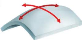
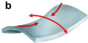
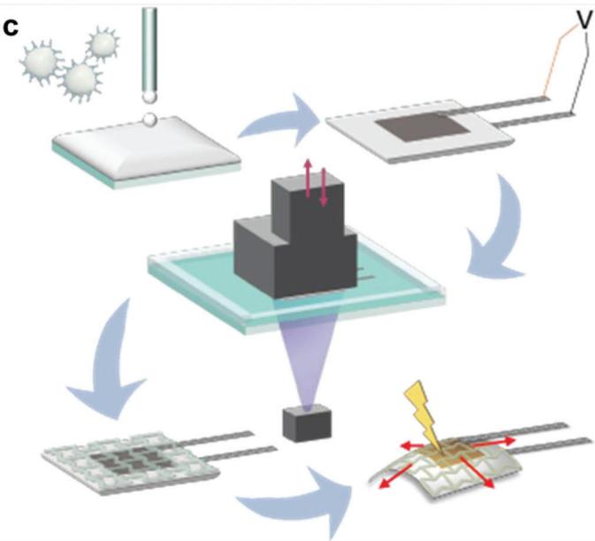
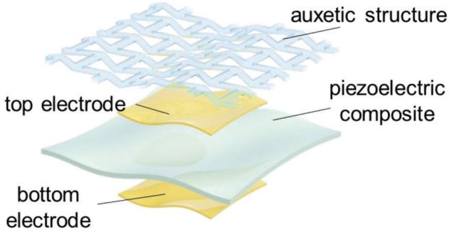
Figure 1. Schematic of a) synclastic and b) anticlastic effect. (c) The fabrication of the auxetic structure-assisted PENG: drop-casting, poling after gold electrodes formation, 3D printing the auxetic structure, and energy harvesting. d) The structure of the auxetic-PENG device.
Structure designing is a promising strategy to overcome the limitations of natural materials. It is found that the repetitive macrostructures can affect various material properties, such as the optical properties, thermal properties, and mechanical properties,[21–23] and are therefore classified as metamaterials. In mechanical metamaterials, auxetic structures are the most widely used structure design, which can achieve a negative Poisson’s ratio that is rarely found in natural materials.[24,25] The most basic auxetic structure consists of a bow-tie structure as a repeating unit, which expands in both the lateral direction and the perpendicular direction to the applied tensile force.[24,26–28] Auxetic strucutre is applied in rigid piezoelectric energy harvesters for enhancing the energy harvesting output via increasing the strain on piezoelectric materials or reducing the frequency range.[29–39] Apart from rigid energy harvesters, auxetic structures also have many applications in the soft electronics field. For example, Jiang et al. developed a carbon nanotube-based piezoresistive sensor with an auxetic structure attached to the sensor film.[40] The auxetic structure can eliminate the Poisson compression that squeezes the active materials, which can effectively enhance the sensitivity and reduce the noise. Fang et al. also reported the PVDF energy harvester with a laser-cut auxetic structure, of which the resonance frequency is reduced due to the larger compliance, and makes it suitable for higher efficiency in low-frequency wind energy harvesting.[41] For all the applications of auxetic structure in soft electronic devices, the planar negative Poisson’s ratio property is used, while the unique property of auxetic structure in the out-of-plane bending, namely, the synclastic effect, has not been exploited. The synclastic effect happens by forming a dome-shaped doubly curved surface when the auxetic material is bent (Figure 1a). On the other hand, an uniform material tends to form a single curved surface under bending, and the materials with hexagonal honeycomb structures tend to form an saddle-shaped surface (Figure 1b).[24]
In this work, taking advantage of the synclastic effect of auxetic structure, a film PENG that can generate electricity in the 3-1 mode under bending is developed with digital light processing (DLP) 3D printing of the auxetic structure (Figure 1c). This unprecedented approach allows auxetic-PENG to harvest energy in the bending mode, which is not possible in typical piezoelectric polymer-based film PENGs. The unique auxetic structure also provides precise control of stretching strain without any overstretching. It can serve as a bending motion sensor for human motion monitoring.
2. Results and Discussion
The structure of the auxetic-assisted PENG (Figure 1d) consists of four layers, namely, the bottom electrode, piezoelectric material, top electrode, and auxetic structure. The piezoelectric film can be fabricated with many methods, including 3D printing, as discussed in our previous report.[42] In this work, the drop-casting method is used to fabricate the piezoelectric layer, after which the gold electrodes are deposited by sputter coating. Then, the auxetic structure was deposited by DLP 3D printing of aliphatic urethane diacrylate to form a firm adhesion layer to the piezoelectric film with the electrodes. The printed auxetic structure is expected to guide the in-plane stretching deformation of the piezoelectric device under bending.
PVDF-based piezoelectric polymer is considered for its largest piezoelectricity among all piezoelectric polymers and their good flexibility. The piezoelectricity in PVDF originates from the positive and negative charge separation in the polymeric chains, which created a metastable ?? phase at room temperature. Copolymer systems are used to enhance the phase crystallization, for example, poly(vinylidene fluoride trifluoroethylene) (P(VDF-TrFE), which enhances the piezoelectric coefficients. Adding piezoelectric ceramic barium titanate nanoparticles (BTO NPs) in the P(VDF-TrFE) matrix can further enhance the piezoelectric coefficient by coupling effect.[42] However, a long-time ultrasonic process is required to uniformly disperse the BTO NPs in the P(VDF-TrFE) solution, and BTO NPs tend to precipitate after several hours. Additionally, at a high particle loading, there are defects that cause the breakdown in the poling process and severely affect the piezoelectricity of the material.[42]
Silane coupling agents are usually used for particle surface modification of oxides. In this work, surface treatment of BTO NPs was carried out with 3-(trimethoxysilyl)propyl methacrylate (TMSPM) for better dispersion and bonding of the particles to the P(VDF-TrFE) matrix. TMSPM is a molecule with a methoxy group that can react with the BTO NPs via hydroxyl dehydration condensation reaction to form a covalent bond and crosslinked structure on the particle surface.[43,44] In addition, the surface modification of BTO NPs show better dispersion and longer precipitation time due to the strong hydrogen bond formed between H and F atom in the matrix.[45,46] 20 wt% TMSPM-surfacemodified BTO NPs (M-BTO NPs) are added into the P(VDF-TrFE) matrix. During the film preparation, 70 mg mL−1 M-BTO/P(VDF-TrFE) was dispersed in dimethylformamide (DMF), cast on glass slides and heated to for solvent evaporation. At the same time, BTO/P(VDF-TrFE) with 20 wt% BTO, and pure P(VDF-TrFE) samples are prepared with the same processes and conditions to serve as a reference to evaluate the effect of TMSPM surface.
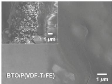
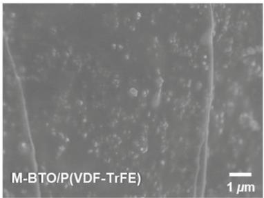
First, the dispersion of the NPs in the matrix is studied with a scanning electron microscope (SEM) as shown in Figure S1a (Supporting Information) and Figure 2a,b. From the SEM result, without the surface modification on BTO NPs, aggregation of the particles occurs (Figure 2a inset), which causes the nonuniformity in the composite that can affect the mechanical and the dielectric property. By contrast, the M-BTO/P(VDF-TrFE) sample shows a perfect dispersion of the particles in the matrix without any ultrasonic treatment of the solution (Figure 2b). The good dispersion with M-BTO is also indicated by the stability of the ink. The M-BTO/P(VDF-TrFE) ink does not separate into clear layer and white layer after weeks, unlike what happens in the BTO/P(VDF-TrFE) ink. The M-BTO/P(VDF-TrFE) drop-cast sample appears in a more whitish color than the BTO/P(VDF-TrFE) sample that is semitransparent, indicating the uniform dispersion of the white BTO NP.
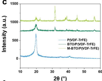
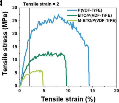
The crystalline structure information can be examined by ray diffractometer (XRD). In Figure S1b of the Supporting Information, the split of the peaks at indicates both the original BTO NPs and the M-BTO NPs are in the piezoelectric tetragonal phase,[47] showing the surface modification does not affect the crystallization of the nanoparticles. The peak at 20° in Figure 2c suggests the original drop-casted and annealed P(VDF-TrFE) is in the piezoelectric ?? phase, and it also shows that after adding the BTO or M-BTO, the number and position of the peaks are the same as the sum of the peaks of the single BTO or M-BTO and P(VDF-TrFE) samples, indicating the piezoelectric phases in the materials are not affected by compositing. Due to the microstructure and crystal phase difference, the mechanical properties of the piezoelectric composite of the three compositions are different, which is examined by tensile testing (Figure 2d). The P(VDF-TrFE) has the largest tensile strength, but after adding BTO NPs and surface-modified BTO NPs, the stress and the strain at breakage are reduced. For all three materials, linear elastic deformation happens at low stress, and after the yield point, nonlinear plastic deformation happens. The yield strain is 2.5%, 2.0%, and 1.5%, for P(VDF-TrFE), BTO/P(VDF-TrFE), and M-BTO/P(VDF-TrFE), respectively. To avoid plastic deformation, the working tensile strain of the PENG should be controlled to be smaller than the yield strain of the piezoelectric material.
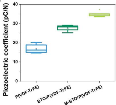
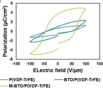
Piezoelectric, ferroelectric, and dielectric properties of the three compositions of samples are tested. The piezoelectric coefficient was tested on the poled samples (Figure 2e), showing that by compositing with BTO NPs, the mean value of the piezoelectric coefficient increases from 17 to 27 pC . While with M-BTO NPs, the piezoelectric coefficient further increased to 35 pC , which is twice that of the pure P(VDF-TrFE). To figure out the reason for the high piezoelectric coefficient of the M-BTO/P(VDF-TrFE) sample, the polarization-electric field loop (P-E loop) is tested to evaluate the polarization process in the samples (Figure 2f). During the test, the remanence polarization of the M-BTO/P(VDF-TrFE) sample is around two times larger than the other samples, and the saturation polarization is also the largest, meaning more internal polarization can be achieved in this material under the same poling electric field. The behavior of a dielectric material under an electric field also depends on the dielectric constant, and the dielectric constant of the samples is tested (Figure S1c, Supporting Information). The result shows that the mean value of the P(VDF-TrFE), BTO/P(VDF-TrFE), and M-BTO/P(VDF-TrFE) samples, the dielectric constant is slightly incremental, which is 14.9, 15.0, and 15.2, respectively.
According to the characterizations above, although there is a reduction in the mechanical properties, the M-BTO/P(VDF-TrFE) composition has an obvious improvement in the ink dispersion, piezoelectricity, ferroelectricity, and dielectric property, comparing with the composite with nontreated particles. Therefore, it was chosen as the piezoelectric composite ink for the device fabrication. Herein, we propose to use the synclastic effect of auxetic structure to achieve energy harvesting by bending on the film PENG. In this way, the energy harvesting mechanism under bending can be transformed to the stretching deformation on the whole piezoelectric film, by the synclastic effect of the 3D printed auxetic structure. The strain on the piezoelectric film is highly increased, and the 3-1 mode piezoelectric effect can be utilized for bending energy harvesting, overcoming the limit of application in the flexible polymer film PENGs.
Simulations were conducted to verify the presence of the synclastic effect on the auxetic structure, the effect of auxetic structure on the stretching deformation of the piezoelectric film, and the stress distribution on the piezoelectric film. The maximum strain on the piezoelectric film under bending can be estimated. The material properties in the finite element analysis (FEA) software COMSOL are set according to the experimental measurement of the real materials (Table S1, Supporting Information), in which the measurement is explained in detail in Section S1 of the Supporting Information.
a
natural_image
Microscopic image showing surface texture with scale bars (1 μm) and label ‘BTO/P(VDF-TrFE)’ indicating material composition (no readable text or symbols beyond labels)
b
natural_image
Microscopic image of a material surface with scale bar indicating 1 μm (no text or symbols on the main subject)
C
line chart
| 2θ (°) | P(VDF-TrFE) | BTO/P(VDF-TrFE) | M-BTO/P(VDF-TrFE) |
|---|---|---|---|
| 10 | ~0 | ~0 | ~0 |
| 20 | ~700 | ~900 | ~1000 |
| 30 | ~0 | ~0 | ~1500 |
| 40 | ~0 | ~0 | ~1000 |
| 50 | ~0 | ~0 | ~1000 |
| 60 | ~0 | ~0 | ~1000 |
d
line chart
| Tensile strain (%) | P(VDF-TrFE) | BTO/P(VDF-TrFE) | M-BTO/P(VDF-TrFE) |
|---|---|---|---|
| 0 | 0 | 0 | 0 |
| 5 | 25 | 12 | 5 |
| 10 | 27 | 13 | 0 |
| 15 | 15 | 0 | 0 |
| 20 | 0 | 0 | 0 |
e
box plot
| Group | Piezoelectric coefficient (pC/N) |
|---|---|
| P(VDF-TrFE) | 15.0 |
| BTO/P(VDF-TrFE) | 28.0 |
| M-BTO/P(VDF-TrFE) | 35.0 |
line chart
| Electric field (V/μm) | P(VDF-TrFE) | BTO/P(VDF-TrFE) | M-BTO/P(VDF-TrFE) |
|---|---|---|---|
| -150 | -2.0 | -3.0 | -5.0 |
| -100 | -1.0 | -2.0 | -4.0 |
| -50 | 0.0 | -1.0 | -3.0 |
| 0 | 1.0 | 0.0 | -2.0 |
| 50 | 2.0 | 1.0 | -1.0 |
| 100 | 3.0 | 2.0 | 0.0 |
| 150 | 4.0 | 3.0 | 1.0 |
g
text_image
g L y z x L L1 θ y z x Φtₐ L₁ ΦwM
h
heatmap
| x | y | Value (×10⁻³) |
|---|---|---|
| 0 | 0 | 0 |
| 0 | 1 | 5 |
| 0 | 2 | 10 |
| 0 | 3 | 15 |
| 0 | 4 | 20 |
| 0 | 5 | 15 |
| 0 | 6 | 10 |
| 0 | 7 | 5 |
| 0 | 8 | 0 |
| 1 | 0 | 0 |
| 1 | 1 | 5 |
| 1 | 2 | 10 |
| 1 | 3 | 15 |
| 1 | 4 | 20 |
| 1 | 5 | 15 |
| 1 | 6 | 10 |
| 1 | 7 | 5 |
| 1 | 8 | 0 |
| 2 | 0 | 0 |
| 2 | 1 | 5 |
| 2 | 2 | 10 |
| 2 | 3 | 15 |
| 2 | 4 | 20 |
| 2 | 5 | 15 |
| 2 | 6 | 10 |
| 2 | 7 | 5 |
| 2 | 8 | 0 |
| 3 | 0 | 0 |
| 3 | 1 | 5 |
| 3 | 2 | 10 |
| 3 | 3 | 15 |
| 3 | 4 | 20 |
| 3 | 5 | 15 |
| 3 | 6 | 10 |
| 3 | 7 | 5 |
| 3 | 8 | 0 |
| 4 | 0 | 0 |
| 4 | 1 | 5 |
| 4 | 2 | 10 |
| 4 | 3 | 15 |
| 4 | 4 | 20 |
| 4 | 5 | 15 |
| 4 | 6 | 10 |
| 4 | 7 | 5 |
| 4 | 8 | 0 |
| 5 | 0 | 0 |
| 5 | 1 | 5 |
| 5 | 2 | 10 |
| 5 | 3 | 15 |
| 5 | 4 | 20 |
| 5 | 5 | 15 |
| 5 | 6 | 10 |
| 5 | 7 | 5 |
| 5 | 8 | 0 |
| z | y | ×10⁻³ |
| x | z | ×10⁻³ |
heatmap
| x | y | z | x (×10⁻³) | y (×10⁻³) |
|---|---|---|---|---|
| 0 | 0 | 0 | -6 | 4 |
| 1 | 0 | 1 | -5 | 3 |
| 2 | 0 | 2 | -4 | 2 |
| 3 | 0 | 3 | -3 | 1 |
| 4 | 0 | 4 | -2 | 0 |
| 5 | 0 | 5 | -1 | -1 |
| 6 | 0 | 6 | 0 | -2 |
| 7 | 0 | 7 | 1 | -3 |
| 8 | 0 | 8 | 2 | -4 |
| 9 | 0 | 9 | 3 | -5 |
| 10 | 0 | 10 | 4 | -6 |
| 11 | 0 | 11 | 5 | -7 |
| 12 | 0 | 12 | 6 | -8 |
| 13 | 0 | 13 | 7 | -9 |
| 14 | 0 | 14 | 8 | -10 |
| 15 | 0 | 15 | 9 | -11 |
| 16 | 0 | 16 | 10 | -12 |
| 17 | 0 | 17 | 11 | -13 |
| 18 | 0 | 18 | 12 | -14 |
| 19 | 0 | 19 | 13 | -15 |
| 20 | 0 | 20 | 14 | -16 |
| 21 | 0 | 21 | 15 | -17 |
| 22 | 0 | 22 | 16 | -18 |
| 23 | 0 | 23 | 17 | -19 |
| 24 | 0 | 24 | 18 | -20 |
| 25 | 0 | 25 | 19 | -21 |
| 26 | 0 | 26 | 20 | -22 |
| 27 | 0 | 27 | 21 | -23 |
| 28 | 0 | 28 | 22 | -24 |
| 29 | 0 | 29 | 23 | -25 |
| 30 | 0 | 30 | 24 | -26 |
| 31 | 0 | 31 | 25 | -27 |
| 32 | 0 | 32 | 26 | -28 |
| 33 | 0 | 33 | 27 | -29 |
| 34 | 0 | 34 | 28 | -30 |
| 35 | 0 | 35 | 29 | -31 |
| 36 | 0 | 36 | 30 | -32 |
| 37 | 0 | 37 |
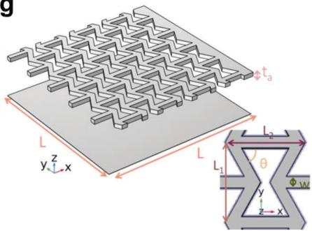
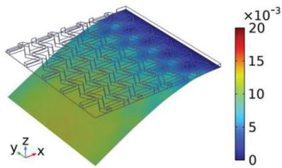
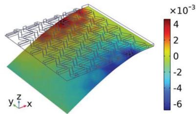
Figure 2. The SEM image of the cross-section of a) BTO/P(VDF-TrFE) (inset is taken at different position of the same sample, showing aggregates of BTO particles), and b) M-BTO/P(VDF-TrFE) films. c) The XRD graph of pure P(VDF-TrFE), BTO/P(VDF-TrFE), and M-BTO/P(VDF-TrFE) films. d) Tensile testing of the P(VDF-TrFE), BTO/P(VDF-TrFE), and M-BTO/P(VDF-TrFE) films. The e) piezoelectric coefficient and f) P–E loop of the pure P(VDF-TrFE), BTO/P(VDF-TrFE), and M-BTO/P(VDF-TrFE) films. g) The 3D model of the auxetic-PENG for finite element analysis. Simulation result of h) X-direction displacement and i) Y-direction displacement (unit: mm).
The 3D models in the FEA have the same dimension and shape as the sample (Figure 2g). A normal bending process involves the moving of two ends and the arch of the middle part. In this way, the direction of the force on the two ends relative to the sample’s longitudinal direction keeps changing. To simplify this process, a cantilever-type bending was used, where one end of the sample is fixed, and a certain displacement is exerted on opposite end of the sample. When the sample with auxetic (5 unit cells along Y-direction) structure is bent to 7 mm in −Z-direction on the −X-edge (opposite to the fixed +X-edge), the local displacements along X- and Y-directions on the piezoelectric film are analyzed (Figure 2h,i) to study the synclastic effect on the sample. Under the cantilever type bending, positive displacement is found on the piezoelectric film at +Y-direction, and negative displacement is found on the piezoelectric film at −Y-direction (Figure 2i), indicating the increase of the overall width along Y-axis (by the distance between the new positions of the two edges) and the expanding of the piezoelectric film in the −Y-direction. The expansion along Y-axis confirms the synclastic effect of the auxetic structure and this expansion has been effectively transferred to the piezoelectric film to guide the in-plain stretching of the film. The X- and Y-direction stress on the piezoelectric film are also analyzed (Figure S3a,b, Supporting Information). The stress on each auxetic void throughout the piezoelectric film is very similar, meaning the stress can be relatively uniformly distributed throughout the whole film sample rather than concentrated on the clamping line.
line chart
| Time (s) | Auxetic Voltage (V) | Non-auxetic Voltage (V) |
|---|---|---|
| 0 | ~1.0 | ~0.0 |
| 1 | ~-1.0 | ~0.0 |
| 2 | ~1.0 | ~0.0 |
| 3 | ~-1.0 | ~0.0 |
| 4 | ~1.0 | ~0.0 |
| 5 | ~-1.0 | ~0.0 |
| 6 | ~0.0 | ~0.0 |
| 7 | ~0.0 | ~0.0 |
| 8 | ~0.0 | ~0.0 |
| 9 | ~0.0 | ~0.0 |
| 10 | ~0.0 | ~0.0 |
line chart
| Time (s) | Forward connection (V) | Inverse connection (V) |
|---|---|---|
| 0.0 | 0.0 | 0.0 |
| 0.25 | 1.0 | -1.0 |
| 0.5 | -1.0 | -1.0 |
| 0.75 | 0.0 | 0.0 |
| 1.0 | 0.0 | 0.0 |
| 1.25 | 0.0 | -1.0 |
| 1.5 | 0.0 | 1.0 |
| 1.75 | 0.0 | 0.0 |
line chart
| Load resistance (Ω) | Voltage (V) | Current density (μA/cm²) |
|---|---|---|
| 1E+3 | 1.5 | 0.0 |
| 1E+4 | 1.2 | 0.0 |
| 1E+5 | 1.0 | 0.0 |
| 1E+6 | 0.8 | 0.0 |
| 1E+7 | 0.6 | 0.04 |
| 1E+8 | 0.4 | 0.08 |
| 1E+9 | 0.2 | 0.1 |
line chart
| Load resistance (Ω) | Power density (μW/cm²) |
|---|---|
| 1E+3 | 0.003 |
| 1E+4 | 0.004 |
| 1E+5 | 0.002 |
| 1E+6 | 0.003 |
| 1E+7 | 0.024 |
| 1E+8 | 0.036 |
| 1E+9 | 0.035 |
line chart
| Prescribed curvature (mm) | Calculated voltage (V) |
|---|---|
| 5 | 2.2 |
| 9 | 1.8 |
| 13 | 1.4 |
| 17 | 1.0 |
| 21 | 0.6 |
line chart
| Curvature (mm) | Output voltage (V) |
|---|---|
| 5 | 1.8 |
| 9 | 1.6 |
| 13 | 1.4 |
| 17 | 1.0 |
| 21 | 0.6 |
line chart
| Time (s) | Voltage (V) |
|---|---|
| 0 | -0.5 |
| 5 | -0.5 |
| 10 | -0.5 |
| 15 | -0.5 |
| 20 | -0.5 |
| 25 | -0.5 |
line chart
| Time (s) | Current density (μA/cm²) |
|---|---|
| 0 | ~0.03 |
| 5 | ~0.04 |
| 10 | ~0.05 |
| 15 | ~0.04 |
| 20 | ~0.06 |
| 25 | ~0.05 |
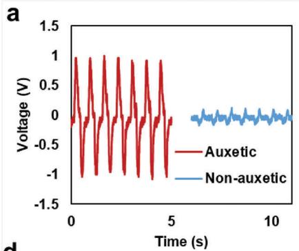
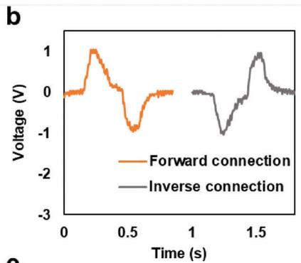
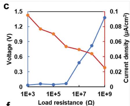
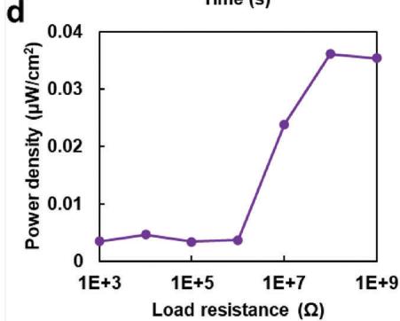
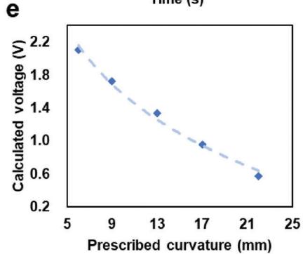
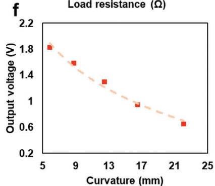
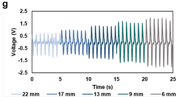
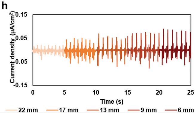
Figure 3. a) The output voltage of the auxetic-PENG and PENG without auxetic structure under 5 mm bending displacement (17 mm bending curvature) and 1.5 Hz frequency. b) Output voltage of bending the auxetic-PENG to 5 mm edge displacement measured by forward connection and inverse connection of the oscilloscope. c) Output voltage, output current density, and d) output power density of the auxetic-PENG with load resistances from 1 kΩ to 1 GΩ at 5 mm bending displacement and 1.5 Hz frequency. e) The calculated and experimental f) output voltage on the piezoelectric film at different prescribed −Z-bending displacement, which is plotted after converting to curvature. The g) output voltage and h) current density of the auxetic-PENG with bending edge displacement from 3 to 11 mm, which is plotted after converting to curvature from 22 to 6 mm.
Since the piezoelectric film is flexible but not stretchable, the maximum strain under bending is studied to see if the stretching on the film exceeds its elastic region (Figure S3c, Supporting Information). With 11 mm −Z-displacement on the edge, the surface average 1st principal strain to be 0.12%, and the larger local strain on the piezoelectric film appears at the edge of the void area of the auxetic structure, where the piezoelectric film is not overlapped with the auxetic layer, to be ≈1%, which is smaller than the yield strain of the M-BTO/P(VDF-TrFE) that is ≈1.5% (Figure 2d). In order to further confirm that the bending with auxetic structure will not cause a strain that is larger than the yield strain of the piezoelectric composite film, experiments were done to examine the real overall in-plain strain on the heavily bent piezoelectric film to be 0.24%, as explained in Section S2 of the Supporting Information. With both the simulation and experimental results, it can be concluded that by using the auxetic structure to assist the stretching of the piezoelectric film, the maximum strain can be controlled at a low value to avoid damage of the device via stretching.
To experimentally study the synclastic effect-induced bending mode energy harvesting of the auxetic-PENG, a sample was bent in the cantilever bending way with one edge clamped and the opposite end pushed with a linear motor at 5 mm displacement (17 mm curvature on the sample) and the generated voltage was measured to be ≈1 V (Figure 3a, red line). Then the auxetic structure was peeled off and the same measurement was done on the M-BTO/P(VDF-TrFE) film without the auxetic structure, resulting in the output voltage to be ≈0.12 V (Figure 3a, blue line), which is 8.3 times smaller than the auxetic-PENG. Since there is a possibility that the output signal is from the triboelectric effect, the moving probe of the shaker was grounded and the measured output voltage of the PENG forward and inverse connected to the oscilloscope was compared. Figure 3b shows that the voltage signal measured by forward and inverse connection has the same value and opposite peak form, meaning that the measured results in this work consist of only the signal from the piezoelectric effect. To find the best working condition of the device, load resistances from 1 kΩ to 1 GΩ are connected in parallel with the PENG, then the output voltage and current density are tested with 5 mm bending displacement (17 mm curvature) and 1.5 Hz frequency, as shown in Figure 3c. The output voltage decreases with increasing load resistance, and the output current density increases with increasing load resistance. The maximum instant output power density is obtained by multiplying the output voltage and the output current density, as shown in Figure 3d. The maximum power density at 5 mm bending displacement (17 mm curvature) and 1.5 Hz frequency is 36 nW cm−2 when the load resistance is 100 MΩ. To study the sensing properties by bending on the auxetic-PENG, different displacement from 3 to 11 mm on the −Z-direction is applied on the edge of the structure, which causes a curvature of the PENG from 22 to 6 mm, and the voltage generated by piezoelectricity is calculated from the simulated volume average stress (Section S3, Supporting Information). The result shows that the output voltage is proportional to the bending displacement (Figure S5a, Supporting Information) and has a quadratic relationship with the bending curvature (Figure 3e). When the bending displacement is 3, 5, 7, 9, and 11 mm (22, 17, 13, 9, and 6 mm curvature, respectively), the absolute value of the calculated output voltage is 0.57, 0.96, 1.34, 1.72, and 2.10 V, respectively. The predictable relationship between output voltage and curvature indicates its potential to be a sensor.
Then experiments were done on the auxetic-PENG sample by bending the sample to the same displacement as the simulation. The output voltage is 0.64, 0.88, 1.24, 1.58, and 1.83 V, at the 22, 17, 13, 9, and 6 mm curvature (3 to 11 mm bending displacement), respectively, as shown in Figure 3f,g and Figure S5b (Supporting Information), which has the same proportional relationship with bending displacement and quadratic relationship with the bending curvature, and similar value compared to the simulated value. The output current density is also tested for the M-BTO/P(VDF-TrFE) samples at different bending displacement (Figure 3h), showing that the current density also increases with the larger bending displacement and smaller curvature, which is 16, 40, 59 71, and 82 nA cm−2 with 22, 17, 13, 9, and 6 mm bending curvature respectively (3 to 11 mm bending displacement).
As the in-plane tensile strain on the piezoelectric film is caused by the synclastic effect of the attached auxetic structure, the shape factor of the auxetic structure should influence the magnitude of the in-plane strain on the piezoelectric film. To study the auxetic structure size effect on the piezoelectric film in-plane strain, simulation and experiments are done. In the simulation, 3, 5, 7, and 9 auxetic repeating units along the Y-direction, with the same thickness along Z-direction are attached onto the piezoelectric film (Figure S5c–f, Supporting Information) and the volumetric strain on the piezoelectric film is analyzed, as shown in Figure 4a,d. The material properties and the mechanical conditions are all set the same as in the simulation above. From the simulated strain distribution, it can be concluded that the finer the auxetic structure, the more uniform the strain is on the film. The output voltage generated by the bending with differentsized auxetic structures are also calculated from the volume average stress (Section S3, Supporting Information) and plotted in Figure 4e. When there is 3-unit large auxetic structure, the calculated voltage is 1.45 V at 7 mm bending displacement, and when the number of auxetic units increases to 5, 7, and 9, the calculated output voltage decrease to 1.34, 1.27, and 1.17 V, respectively. A fine auxetic structure leads to lower output voltage, which may because the less concentrated strain at local areas. The auxetic effect in the fine structure may suffer from more constraint by the larger number of neighboring structures. Additionally, the relationship between the output voltage and bending curvature is analyzed by calculation. The output voltage of devices with auxetic structures in all sizes has a linear relationship versus the bending displacement theoretically (Figure S5g, Supporting Information), and the relationship is quadratic when the bending displacement is converted to curvature (Figure 4f).
Experiments are done with two sizes of auxetic structures to verify the simulation result. Output voltage of the auxetic-PENG with 3, 5, 7, and 9 auxetic units are bent to displacements from 3 to 11 mm (bending curvature 22 to 6 mm) and the output voltage from the PENG is measured by an oscilloscope (Figures 3g and 4g-i). For the PENG with 5-unit auxetic structure (4 mm auxetic unit cell, 5 units), the output voltage increases from 0.64 to 1.83 V when the bending displacement increases from 3 to 11 mm (bending curvature from 22 to 6 mm) as shown in Figure 3g. The sensitivity is 0.154 V mm−1 by bending displacement. When the auxetic structure is larger (6.7 mm auxetic cell, 3 units), the output voltage increases to 0.71–2.02 V and the sensitivity increased to 0.165 V mm−1 for the same bending curvature range, while for the PENG with smaller auxetic structure (2.9 mm auxetic unit cell, 7 units) at the same bending condition, the output voltage decreases to 0.55–1.73 V with bending displacement 3–11 mm. For even a smaller auxetic structure (2.2 mm auxetic unit cell, 9 units), the output voltage further decreases to 0.45–1.49 V. The sensitivity also decreases slightly to 0.148 and 0.125 V mm−1 (7 and 9 auxetic units, respectively) with the increase of auxetic units and decrease of auxetic unit structure size, as shown in Figure S5h of the Supporting Information. The trend is the same as the simulation that smaller auxetic units cause a lower output voltage and slightly lower sensitivity on the piezoelectric film. Compared with other piezoelectric bending sensors (Table S3, Supporting Information), the PENG bending sensor in this work has the highest bending sensitivity and continuous predictable relationship between voltage and curvature due to the auxetic structure enhanced stress on the piezoelectric film.
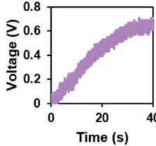
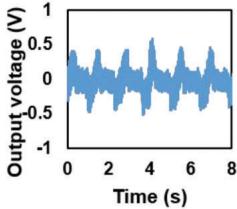
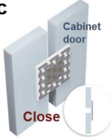
To demonstrate the possible applications of the auxetic-PENG, an auxetic-assisted M-BTO/P(VDF-TrFE) sample was used to power a 1 μF capacitor by bending (5 mm displacement, 1.5 Hz frequency) after rectification with a bridge rectifier (Figure 5a). The capacitor is fully charged in 32 s, showing the energy harvesting function of the auxetic-PENG. Most nanogenerators working with bending motion utilize the stretching on the nanogenerator by attaching it on the outer surface of the bending object. Different from the existing nanogenerators, this auxetic-PENG can harvest energy from bending objects by attaching to the inner surface of the bending object because the mechanism is the synclastic effect rather than the large stretching on the device, which avoids the repetitive overstretching and damage of the sensor at the outer surface of the bending object. With much less stretching strain on the sensor, less fatigue and a longer lifetime can be expected. Additionally, materials selection can be broadened where flexible materials without high stretchability are able to be used as bending sensors. This also provides more options for the bending nanogenerator or sensor to be applied in all the conditions such as when the outer surface is not suitable for attaching sensors. As shown in Figure 5b-d, the auxetic-PENG was mounted on the outer surface of a cabinet door to demonstrate the energy harvesting from the door-open/close motions as a bendable sensor.
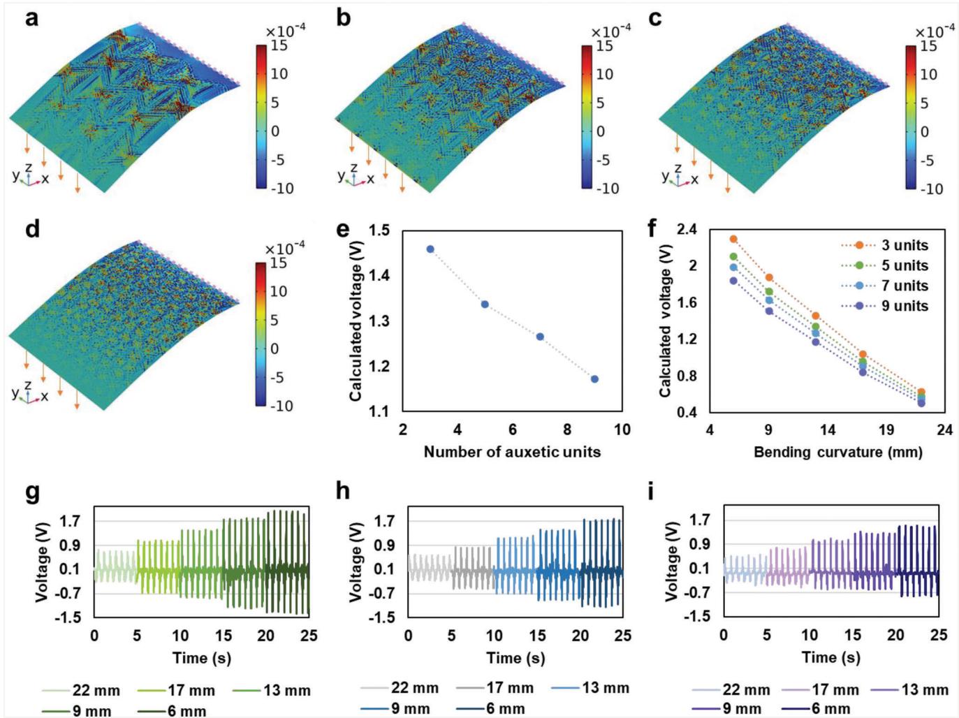
Figure 4. Simulated volumetric strain of the auxetic-PENG with a) 3 units, b) 5 units, c) 7 units, and d) 9 units of auxetic structure. The purple dashed line indicates the fixed constraint on the edge in X-direction, and the orange arrows represent the prescribed displacement on the -X-edge. e) Calculated output voltage of auxetic-PENG with different number of auxetic units under 7 mm bending displacement. f) Calculated output voltage of auxetic-PENG with different number of auxetic units and different bending curvatures. Experimental output voltage of auxetic-PENG with g) 3 auxetic units, h) 7 auxetic units, and i) 9 auxetic units with bending edge displacement from 3 to 11 mm, which is plotted after converting to curvature from 22 to 6 mm (bending frequency 1.5 Hz).
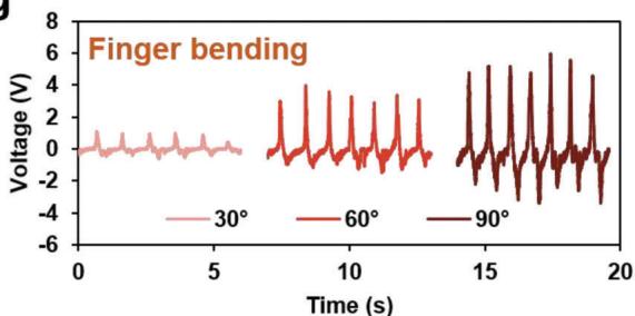
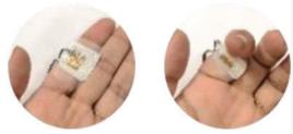
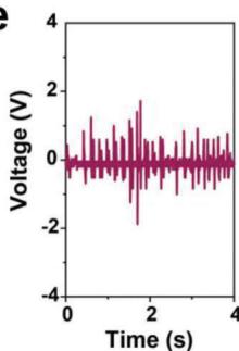
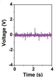
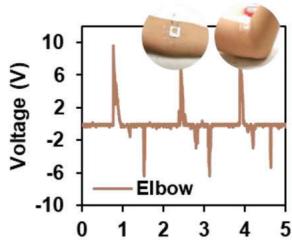
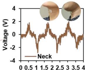
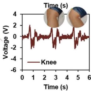
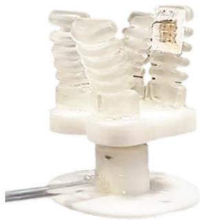
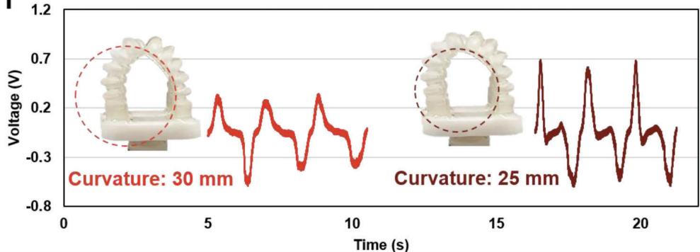
The auxetic-PENG also has the potential to be applied in wind energy harvesting. As a comparison, the auxetic-PENG and the PENG without auxetic structure are tested with a wind tunnel under ≈0.72 m s−1 wind velocity. As shown in Figure 5e,f, the output voltage of the auxetic-PENG is ≈0.8 V. It is four times larger than the output voltage of the PENG without the auxetic structure that is ≈0.2 V. Taking the advantage of the flexibility and sensitivity of the auxetic-PENG, it can be a self-powered sensor for physiological monitoring to sensing human motion by attaching it on the inner side of the joints of the human body that involve bending motion. The auxetic-PENG was attached to the neck, elbow, ankle, knee, and finger of the human body to detect the bending motion at these joints (Figure 5g). In the experiment, the finger is bent to ≈30°, 60°, and 90°, and the output voltage of the auxetic-PENG is ≈1, 3.5, and 5 V, respectively, which shows that the body bending condition can be detected with this auxetic-PENG. Therefore, the auxetic-PENG can be used in selfpowering systems for personal health assessment and medical diagnostics that require monitoring bending angle, such as joint motion monitoring, gait monitoring, etc. The auxetic-PENG can also be a promising candidate for use as a bending sensor in soft robotics due to its output stability, bending signal amplification by the synclastic effect of auxetic structure, lightweight, compliant, and self-powering characteristics, which distinguishes it from the triboelectric, piezoresistive, and capacitive sensors. As shown in Figure 5h, the auxetic-PENG (6.7 mm auxetic cell, 3 units) was attached to a pneumatic soft gripper finger. It provides a real-time feedback on the bending curvature of the gripper finger (Figure 5i; Video S1, Supporting Information). When the bending curvature is 30 mm, the output voltage is ≈0.3 V, and when the bending curvature increases to 25 mm, the output voltage is ≈0.7 V, showing its great potential in smart soft-robots.
a
line chart
| Time (s) | Voltage (V) |
|---|---|
| 0 | 0.0 |
| 10 | 0.3 |
| 20 | 0.5 |
| 30 | 0.65 |
| 40 | 0.7 |
b
line chart
| Time (s) | Output voltage (V) |
|---|---|
| 0 | 0.0 |
| 1 | 0.2 |
| 2 | -0.3 |
| 3 | 0.4 |
| 4 | -0.1 |
| 5 | 0.6 |
| 6 | -0.2 |
| 7 | 0.3 |
| 8 | -0.4 |
g
line chart
| Time (s) | 30° Voltage (V) | 60° Voltage (V) | 90° Voltage (V) |
|---|---|---|---|
| 0 | ~0 | ~0 | ~0 |
| 5 | ~0 | ~0 | ~0 |
| 10 | ~0 | ~4 | ~0 |
| 15 | ~0 | ~5 | ~4 |
| 20 | ~0 | ~5 | ~4 |
text_image
Cabinet door Close
d

text_image
Cabinet door Open
e
line chart
| Time (s) | Voltage (V) |
|---|---|
| 0 | 0 |
| 1 | 0 |
| 2 | 0 |
| 3 | 0 |
| 4 | 0 |
f
line chart
| Time (s) | Voltage (V) |
|---|---|
| 0 | 0 |
| 1 | 0 |
| 2 | 0 |
| 3 | 0 |
| 4 | 0 |
line chart
| Time (s) | Voltage (V) |
|---|---|
| 0 | -2 |
| 1 | 9 |
| 2 | -6 |
| 3 | 7 |
| 4 | -5 |
| 5 | -2 |

natural_image
Silhouette of a running person with orange dots marking specific joints or points (no text or symbols)
line chart
| Time (s) | Voltage (V) |
|---|---|
| 0.0 | 0.0 |
| 0.5 | 2.0 |
| 1.0 | -2.0 |
| 1.5 | 2.0 |
| 2.0 | -2.0 |
| 2.5 | 2.0 |
| 3.0 | -2.0 |
| 3.5 | 2.0 |
| 4.0 | -2.0 |
line chart
| Time (s) | Voltage (V) |
|---|---|
| 0 | 0 |
| 1 | -2 |
| 2 | 0 |
| 3 | -2 |
| 4 | 0 |
| 5 | -2 |
| 6 | 0 |
h
natural_image
Close-up of a white electrical insulator with coiled leads and a base, mounted on a stand (no visible text or symbols)
line chart
| Time (s) | Voltage (V) |
|---|---|
| 0 | -0.3 |
| 5 | 0.2 |
| 10 | -0.3 |
| 15 | 0.7 |
| 20 | -0.7 |
Figure 5. Demonstration of the applications of the PENG. a) The measured voltage of a 1 μF capacitor charged by the fabricated auxetic-PENG. b) Voltage signal generated from the auxetic-PENG during the c) closing and d) opening of a cabinet door, wind energy harvesting with the e) auxetic-PENG, and f) PENG without auxetic structure. g) Demonstration of the applications of the PENG: finger bending angle sensing and body motion sensing of the auxetic-PENG at the neck, elbow, ankle, and knee (IRB-2017-08-038-2). h) A photo of the auxetic-PENG attached on a soft gripper. i) The auxetic-PENG sensing the bending curvature of the soft gripper.
3. Conclusion
In conclusion, an auxetic structure-assisted piezoelectric nanogenerator and sensor based on surface-modified BTO NPs and
P(VDF-TrFE) composite is developed in this work. It was found that the TMSPM modification of BTO NP enhances the piezoelectricity, ferroelectricity, and dielectric constant of the composite, compared with the composite of the nonmodified BTO NP/P(VDF-TrFE), because the more uniform distribution of the modified particles in the P(VDF-TrFE) matrix enhances the force transfer to BTO NP. The synclastic effect of the auxetic structure was applied for the first time to enable the bending energy harvesting mode with the piezoelectric effect in the 3-1 direction, which is not possible on a typical nonstretchable piezoelectric polymer-based film energy harvester. The output voltage and current density at an 11 mm edge displacement in the cantilever-type bending are respectively 1.83 V and 82 nA cm−2. The maximum power output of the auxetic structure-assisted bending piezoelectric nanogenerator can be achieved at 100 MΩ load resistance. The output voltage is linear with bending displacement and quadratic with the bending curvature, showing the sensing ability. The size factor of the auxetic structure is studied by both simulation and experiment showing a finer auxetic structure results in a lower output. The study of the auxetic structure form factors on the bending energy harvesting performance provides a guideline for the optimization and customization of the auxetic-PENG. For application, this auxetic-PENG was demonstrated to be useful as an energy harvester as well as a selfpowered sensor for physiological monitoring for personal health assessment and medical diagnostics.
4. Experimental Section
Materials: BTO NPs (Nanostructured & Amorphous Materials, Inc.) with a diameter of ≈200 nm were surface modified with TMSPM (98%, Sigma-Aldrich) by mixing 1 mL TMSPM, 50 mL ethanol, 1 mL acetic acid, 9 mL deionized water, 1 g BTO NP, sonicating in a bath sonicator (S60H, Elmasonic) for 30 min, and stirring for 24 h. Then, the modified powders were washed with ethanol twice with a centrifuge (Sorvall ST 16, Thermo Scientific) and dried at room temperature. To form a drop-casting solution, P(VDF-TrFE) (70–30 wt%) powders (Piezotech Arkema Group) were mixed into DMF (Sigma-Aldrich) by magnetic stirring for 1 h with a concentration of 70 mg mL−1. Then, the M-BTO NPs were added to the solution accordingly. The mixture was manually stirred for good dispersion. To form a piezoelectric film, the solution was drop-casted on 2 cm × 2 cm glass slides at 80 °C for 1 h and annealed at 120 °C and 2 h for crystallization of P(VDF-TrFE). Then, 1 cm × 1 cm gold electrodes were sputter-coated onto the top and bottom sides of the drop-casted piezoelectric film. The piezoelectric film with electrodes was poled with an amplifier/controller (Trek 610E H.V.) under a 50 V μm−1 electric field at 100 °C. The ink for 3D printing auxetic structure was prepared with 98 wt% oligomers (Ebecryl 8402, Allnex), and 2 wt% photoinitiator diphenyl(2,4,6-trimethylbenzoyl)phosphine oxide (Sigma-Aldrich, 97%, St. Louis, USA) by manual stirring. The Ebecryl 8402 oligomers were chosen because it has good flexibility, toughness, and excellent adhesion to different substrates, so that it can attach to both the piezoelectric material and the electrode well.
Printing: The 3D model of the auxetic structure was built with the software Inventor 2018 (Autodesk, Inc.) and printed with a digital light projection (DLP) 3D printer (Pico 2, Asiga). The drop-casted piezoelectric film with electrodes was stuck as a substrate onto the printing stage with tape. During printing, the ink was filled into the ink container and UV light was projected onto the substrate to selectively cure the oligomer to form an auxetic polymer onto the piezoelectric film. After printing, the sample was wiped with ethanol and exposed to UV with a UV lamp (365 nm wavelength, 40 W, ASG 400, Asiga) for 3 min for full curing.
Characterizations: The crystallographic phase of the materials was characterized by a powder XRD (Shimadzu XRD 7000). The morphology of the materials and samples was characterized with a field-emission SEM (Joel 7600F). The mechanical properties were tested by a mechanical tester (Instron 5567) with tensile extension mode. The longitudinal mode piezoelectric coefficient (d ) of the samples was tested by a standard static piezoelectric constant measuring instrument (Sinocera YE2730). The energy harvesting performances were evaluated by bending the device in the manner shown in Figure S6a–b of the Supporting Information, and analyzing the output signals measured by a customized system, including a function generator (YE 1311, Sinocera), a signal amplifier (YE5878, Sinocera), a magnetic shaker (JZK-20, Sinocera), an oscilloscope (MDO 3024, Tektronix), and an electrometer (6517B, Keithley), with the circuit shown in Figure S6c of the Supporting Information. The load resistance for the measurement of output at different bending curvature is 100 MΩ. The dielectric constant of the samples was measured with a precision impedance analyzer (4294A, Agilent), and the P–E loop was measured with a ferroelectric test system (P-LC and P-HVI4K, Radiant Technologies and 609E-6, Trek). To charge a capacitor using the PENG, the device was connected to a bridge rectifier and then was connected to a capacitor, as shown in Figure S6d of the Supporting Information. For the demonstration of body motion sensing, the device was mounted on the human body with tape. This study was approved by the Institutional Review Board (IRB) at Nanyang Technological University (IRB-2017-08-038-2). Informed signed consent was obtained from all the participants.
Simulation: Finite element analysis was performed to the 3D model using the software COMSOL Multiphysics (COMSOL, Inc.). The electrodes were ignored because the thickness of sputtered gold electrodes was negligible. The contact between the auxetic structure and the piezoelectric film was set to union. Solid mechanics physics was used, and the models were divided into hexahedrons. The Young’s modulus, Poisson’s ratio, relative permittivity, and piezoelectric coefficients d and d of piezoelectric film were obtained from the experiment, as shown in Table S1 of the Supporting Information, and transformed into the elastic matrix and coupling matrix. All the structures were constrained with all degrees of freedom on the right (+X-direction) surface and displacement was applied on the opposite left (−X-direction) surface to all the structures along −Z-direction.
Supporting Information
Supporting Information is available from the Wiley Online Library or from the author.
Acknowledgements
This work was supported by the Campus for Research Excellence and Technological Enterprise (CREATE) that was supported by the National Research Foundation, Prime Minister’s Office, Singapore.
Conflict of Interest
The authors declare no conflict of interest.
Data Availability Statement
The data that support the findings of this study are available from the corresponding author upon reasonable request.
Keywords
3D printing, auxetic, energy harvesters, piezoelectric nanogenerator, wearable electronics
Received: April 18, 2023
Revised: June 28, 2023
Published online: July 16, 2023
[1] A. Proto, M. Penhaker, S. Conforto, M. Schmid, Trends Biotechnol. 2017, 35, 610.
[2] Z. L. Wang, Faraday Discuss. 2014, 176, 447.
[3] K. Parida, J. Xiong, X. Zhou, P. S. Lee, Nano Energy 2019, 59, 237.
[4] J. Briscoe, S. Dunn, Nano Energy 2014, 14, 15.
[5] Z. L. Wang, Mater. Today 2017, 20, 74.
[6] S. Mishra, L. Unnikrishnan, S. K. Nayak, S. Mohanty, Macromol. Mater. Eng. 2019, 304, 1800463.
[7] C. R. Bowen, H. A. Kim, P. M. Weaver, S. Dunn, Energy Environ. Sci. 2014, 7, 25.
[8] V. V. Kochervinskiˇı, Crystallogr. Rep. 2003, 48, 649.
[9] S. Siddiqui, D. Il Kim, L. T. Duy, M. T. Nguyen, S. Muhammad, W. S. Yoon, N. E. Lee, Nano Energy 2015, 15, 177.
[10] S. K. Kim, R. Bhatia, T. Kim, D. Seol, J. H. Kim, H. Kim, W. Seung, Y. Kim, Y. H. Lee, S. Kim, Nano Energy 2016, 22, 483.
[11] B. Kumar, S. W. Kim, Nano Energy 2012, 1, 342.
[12] V. Bhavanasi, V. Kumar, K. Parida, J. Wang, P. S. Lee, ACS Appl. Mater. Interfaces 2016, 8, 521.
[13] S. K. Karan, D. Mandal, B. B. Khatua, Nanoscale 2015, 7, 10655.
[14] H. Kim, F. Torres, Y. Wu, D. Villagran, Y. Lin, T.-L. Tseng, Smart Mater. Struct. 2017, 26, 085027.
[15] Y. Duan, Y. Huang, Z. Yin, N. Bu, W. Dong, Nanoscale 2014, 6, 3289.
[16] F. Jasni, N. A. Hamzaid, A. Gani, A. Muthalif, Z. Zakaria, IEEE/ASME Trans. Mechatronics 2016, 21, 2466.
[17] L. Ruan, X. Yao, Y. Chang, L. Zhou, G. Qin, X. Zhang, Polymers 2018, 10, 228.
[18] Y. Shin, S. Sohn, H. Han, Y. Park, H. Shin, Nano Energy 2020, 72, 104671.
[19] W. Li, Q. Meng, Y. Zheng, Z. Zhang, W. Xia, Z. Xu, Appl. Phys. Lett. 2010, 96, 034105.
[20] X. Zhou, K. Parida, O. Halevi, S. Magdassi, P. S. Lee, Sensors 2020, 20, 6478.
[21] A. Q. Liu, W. M. Zhu, D. P. Tsai, N. I. Zheludev, J. Opt. 2012, 14, 114009.
[22] X. Zheng, H. Lee, T. H. Weisgraber, M. Shusteff, J. DeOtte, E. B. Duoss, J. D. Kuntz, M. M. Biener, Q. Ge, J. A. Jackson, S. O. Kucheyev, N. X. Fang, C. M. Spadaccini, Science 2014, 344, 1373.
[23] J. Christensen, M. Kadic, O. Kraft, M. Wegener, MRS Commun. 2015, 5, 453.
[24] M. Mir, M. N. Ali, J. Sami, U. Ansari, Adv. Mater. Sci. Eng. 2014, 2014, 753496.
[25] D. Vella, Nat. Rev. Phys. 2019, 1, 425.
[26] X. Ren, R. Das, P. Tran, T. D. Ngo, Y. M. Xie, Smart Mater. Struct. 2018, 27, 023001.
[27] E. Khare, S. Temple, I. Tomov, F. Zhang, S. K. Smoukov, Front. Mater. 2018, 5, 45.
[28] S. Chen, S. C. Ryu, Smart Mater. Struct. 2017, 26, 115026.
[29] A. Tabak, B. Safaei, A. Memarzadeh, S. Arman, C. Kizilors, J. Vib. Eng. Technol. 2023, 1, 1.
[30] K. Chen, W. Liao, Proc. SPIE 2023, 2023, 1.
[31] Q. Li, Y. Kuang, M. Zhu, AIP Adv. 2017, 7, 015104.
[32] T. Fey, F. Eichhorn, G. Han, K. Ebert, M. Wegener, A. Roosen, K. I. Kakimoto, P. Greil, Smart Mater. Struct. 2015, 25, 015017.
[33] R. Ichige, N. Kuriyama, Y. Umino, T. Tsukamoto, T. Suzuki, Sens. Actuators, A 2021, 318, 112488.
[34] P. Eghbali, D. Younesian, A. Moayedizadeh, M. Ranjbar, Sci. Rep. 2020, 10, 16338.
[35] P. Eghbali, D. Younesian, S. Farhangdoust, Int. J. Energy Res. 2020, 44, 1179.
[36] K. Chen, Q. Gao, S. Fang, D. Zou, Z. Yang, W. H. Liao, Appl. Energy 2021, 298, 117274.
[37] M. S. Mazloomi, M. Ranjbar, L. Boldrin, F. Scarpa, S. Patsias, N. Ozada, Compos. Struct. 2018, 187, 593.
[38] W. J. G. Ferguson, Y. Kuang, K. E. Evans, C. W. Smith, M. Zhu, Sens. Actuators, A 2018, 282, 90.
[39] S. Farhangdoust, Proc. SPIE 2020, 2020, 1.
[40] Y. Jiang, Z. Liu, N. Matsuhisa, D. Qi, W. R. Leow, H. Yang, J. Yu, G. Chen, Y. Liu, C. Wan, Z. Liu, X. Chen, Adv. Mater. 2018, 30, 1706589.
[41] L. Fang, J. Li, Z. Zhu, S. Orrego, S. H. Kang, J. Mater. Res. 2018, 33, 330.
[42] X. Zhou, K. Parida, O. Halevi, Y. Liu, J. Xiong, S. Magdassi, P. S. Lee, Nano Energy 2020, 72, 104676.
[43] T. Nguyen, T. Nguyen, D. Vu, D. Dinh, A. Nguyen, T. Ly, P. Dao, T. Nguyen, L. Bach, H. Thai, J. Chem. 2020, 2020, 1381407.
[44] B. D. Ratner, A. S. Hoffman, in Biomaterials Science: An Introduction to Materials: Third Edition, Academic Press, Kidlington, Oxford, UK, 2012, pp. 259–276.
[45] P. Shi, Y. Wang, K. Wan, C. Zhang, T. Liu, Adv. Funct. Mater. 2022, 32, 2112293.
[46] B. Yiming, Y. Han, Z. Han, X. Zhang, Y. Li, W. Lian, M. Zhang, J. Yin, T. Sun, Z. Wu, T. Li, J. Fu, Z. Jia, S. Qu, Adv. Mater. 2021, 33, 2006111.
[47] X. Chen, K. Parida, J. Wang, J. Xiong, M.-F. Lin, J. Shao, P. S. Lee, ACS Appl. Mater. Interfaces 2017, 9, 42200.