ENERGY SCAVENGING WITH SHOE-MOUNTED PIEZOELECTRICS
DECREASING SIZE AND POWER REQUIREMENTS OF WEARABLE
MICROELECTRONICS MAKE IT POSSIBLE TO REPLACE BATTERIES WITH
SYSTEMS THAT CAPTURE ENERGY FROM THE USER’S ENVIRONMENT.
UNOBTRUSIVE DEVICES DEVELOPED AT THE MIT MEDIA LAB SCAVENGE
ELECTRICITY FROM THE FORCES EXERTED ON A SHOE DURING WALKING: A
FLEXIBLE PIEZOELECTRIC FOIL STAVE TO HARNESS SOLE-BENDING ENERGY
AND A REINFORCED PZT DIMORPH TO CAPTURE HEEL-STRIKE ENERGY.
Nathan S. Shenck Joseph A. Paradiso MIT Media Laboratory, Responsive Environments Group
Consumer reliance on wearable electronic devices has grown significantly in the past decade. With increasing use come demands for decreased size and enhanced capabilities, necessitating new ways to supply electric energy to these devices. Until now, chemical-cell batteries have been sufficient, but replacing them is a costly nuisance, and this solution will become less practical as demands evolve. Another approach is a centralized, body-worn power pack, with multiple distribution lines, but such a system will be cumbersome and impractical as the user wears more devices.
Fortunately, as power requirements drop for body-worn devices, a third approach, which eliminates the power wiring problem, is emerging: developing and storing electric energy at the devices themselves by scavenging waste energy from human activities. For example, the average person spends a significant part of the day on foot, dissipating abundant energy into the insole of a shoe. Harnessed unobtrusively, this wasted energy could be used in a variety of low-power applications, such as pagers, health monitors, self-powered emergency receivers, radio frequency identification (RFID) tags, and emergency beacons or locators. If wiring devices to the generator proves impractical for some applications, a battery could be trickle-charged at the shoe and manually moved into the devices.
Studies at the MIT Media Laboratory have explored the feasibility of harnessing waste energy from a variety of body sources. Thad Starner’s benchmark conceptual investigation in 1995 analyzed various human activities and found that the heel strike during walking is the most plentiful and readily tapped source of waste energy.1 Starner estimated that 67 watts of power are available in the heel movement of an average (68 kg) person walking at a brisk pace (two steps per second with the foot moving 5 cm vertically). Admittedly, scavenging most of that energy unobtrusively would be impossible. But even a small percentage of it (up to a sizable fraction of a watt),2 removed imperceptibly, would provide enough power to operate many of the bodyworn systems on the market today.
A second MIT Media Lab study3 and independent work at other institutions (for example, Antaki et al.4 ) supported this conclusion and proposed a system of embedded piezoelectric materials and miniature control electronics. The researchers observed that a shoe or boot having a relatively large volume of space available in the sole and the heel platform would make an ideal test bed for exploring body-energy harvesting.
In the years since these studies, researchers have further explored parasitic power harvesting in shoes. In particular, at the MIT Media Lab, we have implemented a demonstration of shoe power at work and developed new ways to efficiently condition raw, lowfrequency piezoelectric shoe signals into a continuous, reliable energy source. Other approaches use rigid piezoelectric materials driven at resonance to achieve higher power levels. In contrast, we have concentrated on embedding simple mechanical structures and flexible piezoelectric materials into the shoe, resulting in minimal impact on the shoe’s design or feel.
text_image
Electrostatic poling direction (across metallized surfaces) Piezoelectric material (a) 3 2 1 Front of shoe Mechanically stressed axis during fabrication
text_image
Expansion strain along 1-axis Metallized piezoelectric laminate Neutral axis Compression strain along 1-axis Metallized piezoelectric laminate View from side of shoe (b) Vout along 3-axis
text_image
Compression strain along 3-axis Piezoelectric element Thickness of heel insole (c)
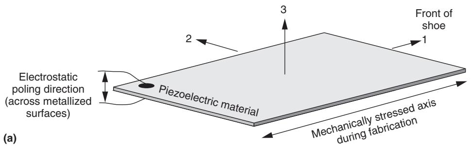
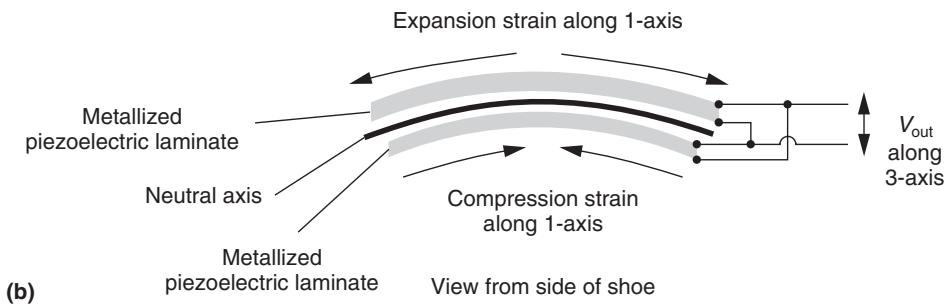
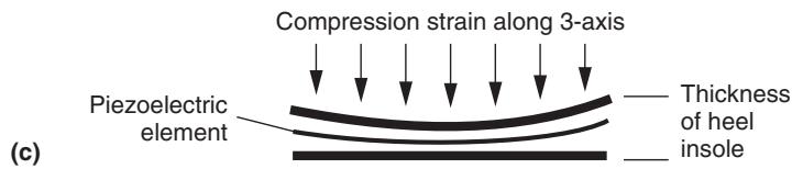
Figure 1. Conventional axis definition for a piezoelectric material (a). Our applications rely on 31- mode (b) in bending. The 33-mode (c)—when the heel motion in the 3-axis direction compresses the shoe’s sole and induces an electric field along the same axis—is intuitively appealing but inefficient because of the small integrated strain across the thickness dimension (3-axis).
Piezoelectric shoe power: two approaches
The piezoelectric effect—a material’s capacity to convert mechanical energy into electrical energy, and the inverse—is observable in a wide array of crystalline substances that have asymmetric unit cells. When an external force mechanically strains a piezoelectric element, these polarized unit cells shift and align in a regular pattern in the crystal lattice. The discrete dipole effects accumulate, developing an electrostatic potential between opposing faces of the element. Relationships between the force applied and the subsequent response of a piezoelectric element depend on three factors: the structure’s dimensions and geometry, the material’s piezoelectric properties, and the mechanical or electrical excitation vector.
To designate direction within a piezoelectric element, engineers conventionally define a three-dimensional, orthogonal modal space, as shown in Figure 1a. The various electromechanical operation modes identify the electrical and mechanical excitation axes: per convention, electrical I/O appears along the first-named i-axis, and its mechanical counterpart appears along the following j-axis. As Figures 1a and 1b show, the top and bottom of the piezoelectric material are metallized, causing the 3-axis to be electrically coupled. During manufacture, the material is “poled” when a high voltage is applied across the 3-axis electrodes at elevated temperature, reordering the unit cells so they produce a voltage across the 3-axis in response to strain across axes 1, 2, or 3.5 For example, 31-mode operation signifies transverse mechanical strain along the 1-axis, inducing an electric field along the 3-axis, as shown in Figure 1b. This action is equivalent to pulling both ends of a ruler, thereby developing a potential difference between the ruled faces.
text_image
Insole PZT dimorph Metal midplate PZT unimorph PZT unimorph PVDF stave Sole
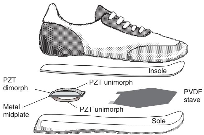
Figure 2. Two approaches to unobtrusive 31-mode piezoelectric energy scavenging in shoes: a PVDF stave under the ball of the foot and a PZT dimorph under the heel.
text_image
(a) 2 1
natural_image
Close-up of a mechanical component with a metallic body and black rectangular body, labeled (b), with an arrow pointing to part 1 (no text or symbols on the object itself)
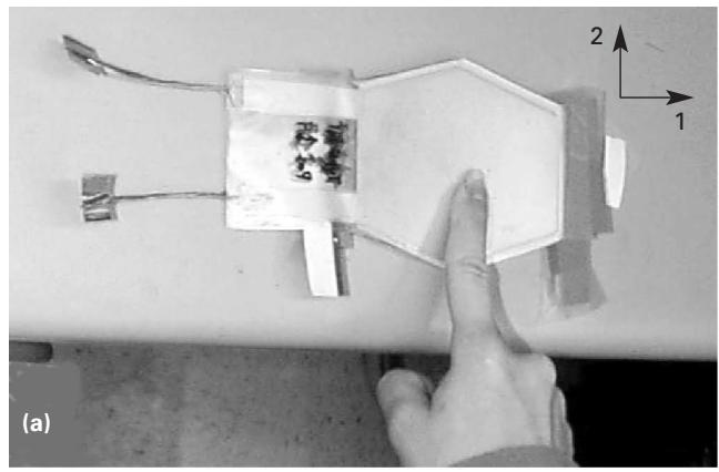
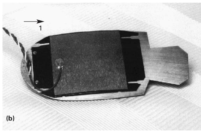
Figure 3. View looking down at the PVDF insole stave (a) and the PZT dimorph heel insert (b). In both views, the right side of the device is pointing to the shoe’s toe.
Piezoelectric materials can be fabricated from crystals, ceramics, or flexible foils. In addition to applications as sensors or input devices (such as this one), piezoelectric materials can be driven with a voltage to produce mechanical deflection, for a wide range of output-device applications.
An insole’s dimensions limit the size and shape of materials that can be integrated into footwear without loss of comfort or a radical change in design. Therefore, a thin, flat piezoelectric element is a natural choice for this application. Commonly, we excite an element of this shape in 31-mode operation by flexing a plate about its neutral axis, inducing compression or extension of the piezoelectric material bonded to the plate’s faces (Figure 1b). Although intuitively attractive, bulk compression under the wearer’s weight (33-mode excitation, as shown in Figure 1c) is impractical because of the typical material and electromechanical properties of inelastic piezoelectrics and the limited forces exerted in walking. Other excitation modes are equally impractical under these constraints. Therefore, we consider 31-mode operation most appropriate for harnessing waste energy in an insole.
We explored two main methods, illustrated in Figure 2, of piezoelectrically scavenging shoe power in bending 31-mode operation. One method is to harness the energy dissipated in bending the ball of the foot, using a flexible, multilaminar polyvinylidene fluoride (PVDF) bimorph stave mounted under the insole. The second method is to harness foot strike energy by flattening curved, prestressed spring metal strips laminated with a semiflexible form of piezoelectric lead zirconate titanate (PZT) under the heel. This device, which we call a dimorph, consists of two backto-back, single-sided unimorphs.
We developed the elongated, hexagonal, multilaminate piezoelectric-foil stave6 in collaboration with Kyung Park and Minoru Toda of the Sensor Products Division of Measurement Specialties (formerly AMP Sensors).The stave consists of two eight-layer stacks of 28-micron PVDF sandwiching a 2-mm flexible plastic substrate bonded with epoxy. The hexagonal design maximizes integrated stress across the bending distribution of a typical insole and conforms to the shoe’s shape (see Figure 3a). Bending the stave elongates its outside surface and compresses its inside surface with respect to its plastic core because of their different curvature radii. The PVDF sheets on either side of the core are connected appropriately so the silver electrodes on each sheet appear in parallel (flipping polarity on opposite sides as in Figure 1b) and the discrete charge accumulations of the 16 layers are additive. A voltage therefore develops across the two leads, supported by the multilaminate structure’s net 330-nF capacitance. Restoring the stave’s shape, as well as bending it, liberates energy if the resulting charge is optimally removed at each relative minimum and maximum deflection in the step cycle.
The second device (Figure 3b) exploits the abundant energy exerted in a heel strike. Although we used a simple unimorph7 in our first model, we later constructed a nonbending, compressible dimorph8 in cooperation with the C.S. Draper Laboratory. It consists of two commercially available PZT transducers, a heel-shaped 0.025-inch beryllium-copper midplate,
and two aluminum rivets. The insert fits snuggly into the heel portion of a hollowed orthopedic insole, and because its volume and compressive flexibility closely match the material removed to accommodate it, its presence is unnoticeable. We incorporated two Thunder TH-6R transducers manufactured by Face International Corp. using a semiflexible piezoceramic manufacturing process developed by NASA Langley in the Rainbow (reduced and internally biased oxide wafer) design project. The transducers consist of a 5 × 5-cm, 0.015- inch PZT strip bonded to a prestressed, neutrally curved, 5 × 8.5-cm sheet of spring steel. We trimmed them to fit the beryllium-copper midplate, mounted them under the heel-strike force center with two rivets, and connected them in electrical parallel. As with the PVDF stave, charge develops across the faces of the PZT strips when the dimorph is compressed or released. Hence, a voltage appears, supported by the source’s net 140-nF capacitance.
line chart
| Time (s) | Volts (mW) |
|---|---|
| 0.5 | 9.8 |
| 1.3 | 1.3 |
line chart
| Time (s) | Volts (mW) - IVI = 44 V | Volts (mW) - = 8.4 mW |
|---|---|---|
| 0 | ~75 | ~10 |
| 1 | ~190 | ~75 |
| 2 | ~180 | ~60 |
| 3 | ~200 | ~80 |
| 4 | ~190 | ~65 |
| 5 | ~10 | ~10 |
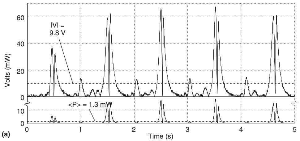
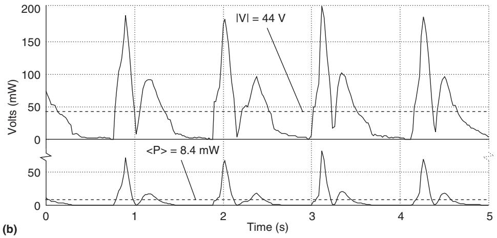
Figure 4. Power and rectified voltage waveforms from brisk-walking tests of optimally loaded PVDF stave (a) and PZT dimorph (b).
Performance
To evaluate and compare the output of the two shoe generators, we installed and tested them. We placed the PVDF stave under the insole of a standard Nike athletic sneaker and the PZT dimorph in an orthopedic insole in a US Navy work boot. We chose these test platforms with the devices’ physical characteristics in mind: The Nike insole’s flexibility accommodated the flexible stave, and the work boot’s rigid heel cup suited the rigid dimorph. Neither device affected the gait, and, with a little padding, both were at most barely perceivable during the wearer’s normal activity. To determine the devices’ approximate raw power and electromechanical efficiency, we terminated the transducers with matched resistive loads and measured their voltage during a brisk walk. Figure 4 (previous page) shows the resulting plots.
natural_image
Black-and-white photo of a Nike running shoe with an electronic circuit board, placed outdoors near a building sign (no readable text on the shoe itself)
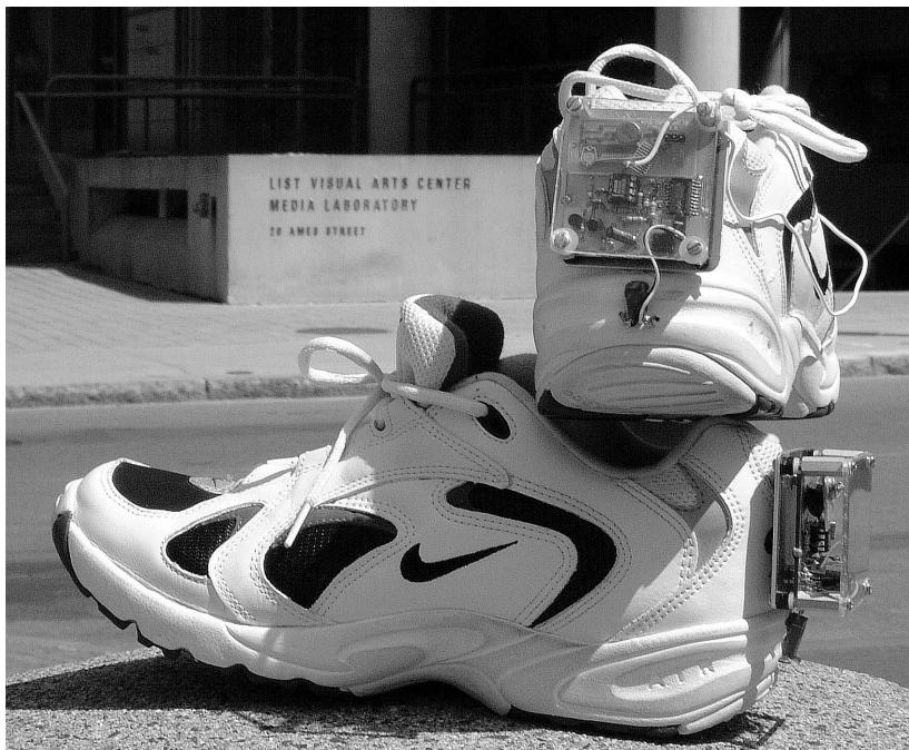
Figure 5. Piezoelectric-powered RFID shoes with mounted electronics.
For the PVDF stave, the average power in a 250-kΩ load at a 0.9-Hz walking pace was 1.3 mW. Conversely, the PZT dimorph produced on average 8.4 mW in a 500-kΩ load under similar excitation. The footfall characteristics are evident in these plots. The larger power spikes correspond to the device’s rapid initial bending or compression, and the following smaller spikes represent transducer restoration when the walker more slowly shifts his weight to the opposite foot. Therefore, both sources alternate polarity with respect to the source ground twice between steps, yielding two distinct current pulses per step cycle. Because of the source voltage’s bipolar nature, rectification is required.
Finally, by comparing the open-circuit voltage across each device’s known static capacitance under a constant test force, we measured the raw electromechanical efficiencies as approximately 0.5 percent for the stave and 20 percent for the dimorph. Further, at low frequencies, the equivalent circuit for both transducers is essentially the device’s static capacitance in parallel with a large resistance for modeling dielectric leakage. This implies that the test force must be applied quickly and the source voltage read immediately to minimize deleterious leakage effects on an accurate approximation of available energy.
Shoe-powered RF tag system
To demonstrate the feasibility and utility of scavenged shoe power, we developed a simple application circuit.7 The design is a self-powered, active radio frequency (RF) tag that transmits a short-range, 12-bit wireless identification (ID) code while the bearer walks. This system has immediate application in a smart environment, in which multiple users transmit their identities to the local surroundings. The IDs, for example, can enable a central server to make dynamic, near-real-time decisions to personalize the environment or route appropriate information to mobile users. Most previous work in this area relied on battery-powered infrared (IR) badges.9 Our RF-based design, however, requires no line of sight to the reader and therefore can be mounted in a shoe, operating without a battery under the power of a piezoelectric insert. Figure 5 shows a functional prototype pair of self-powered RFID sneakers.
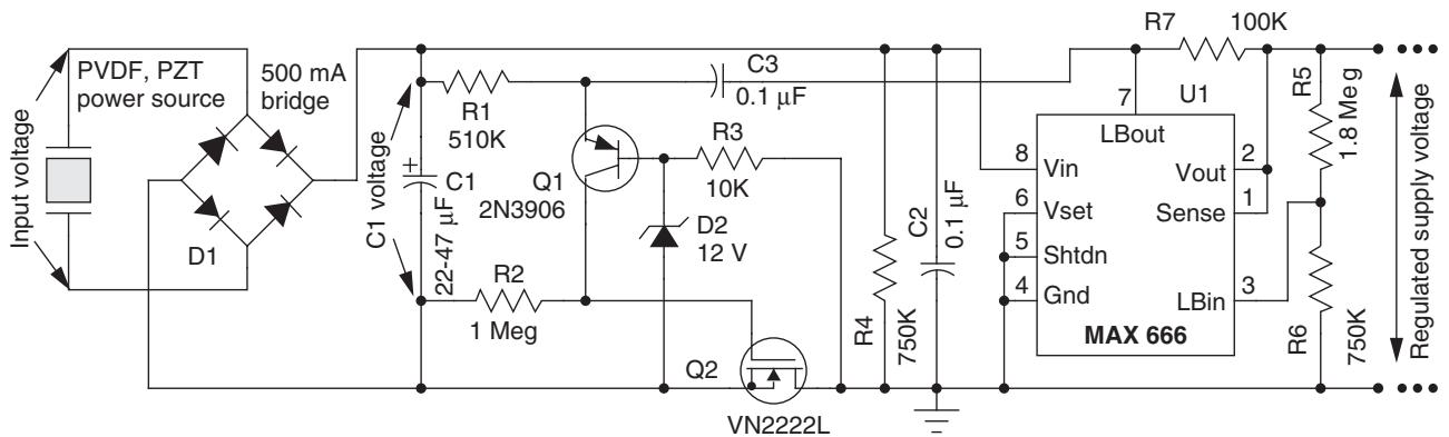
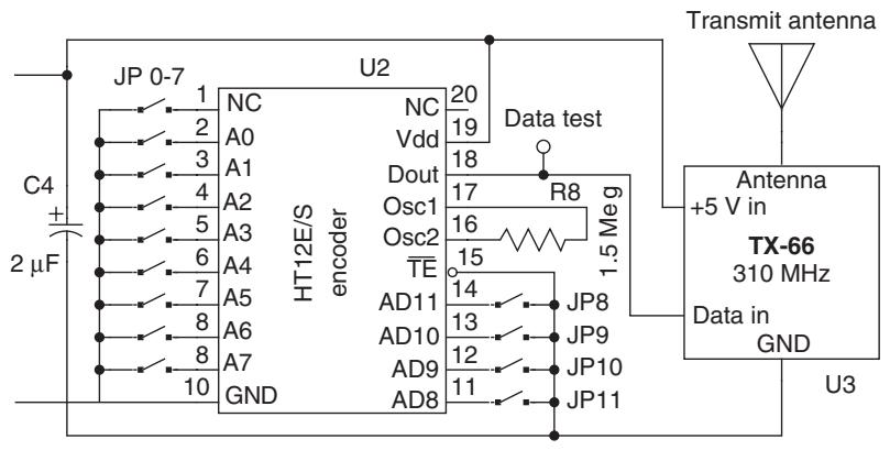
Figure 6 shows the RF tag system schematic. This design uses scavenged energy from either the PVDF or PZT source to encode and transmit a periodic, On/Off-keyed RFID signal using devices developed for automotive keyless entry systems. A local base station receives the transmission and emits an audible chirp upon identifying the transmitter. The signal from the piezoelectric source is full-wave rectified through 500-mA diode bridge D1. As the source signal ramps up, charge transfers to electrolytic bucket capacitor C1 whenever the source voltage overcomes the voltage already supported by this capacitor (plus two diode drops). As C1 charges beyond 12.6 V (the Z1 breakdown voltage plus the diode drop across the base-emitter junction of Q1), Q1 is forced into conduction, in turn activating Q2 and latching Q1. With Q1 on, the high side of C1 now has a current return path to ground and discharges through the Maxim MAX666 low-dropout (LDO) linear regulator U1.
The regulator is biased to provide a stable +5 V to the serial ID encoder U2 and RF transmitter U3, as long as C1 has sufficient charge to produce a valid regulator output voltage . Note that exhibits some ripple when supplying the transmitter during the ID code’s
text_image
PVDF, PZT power source 500 mA bridge C1 voltage D1 R1 510K C1 2N3906 Q1 22-47 µF R2 1 Meg C3 0.1 µF R3 10K D2 12 V Q2 VN2222L C2 750K R4 8 750K C2 0.1 µF R5 1.8 Meg R6 750K L Bout Vin Vset Shtdn Gnd Vout Sense LBin MAX 666 Regulated supply voltage
text_image
JP 0-7 1 NC 2 A0 3 A1 4 A2 5 A3 6 A4 7 A5 8 A6 9 A7 10 GND U2 NC Vdd Dout Osc1 Osc2 TE AD11 AD10 AD9 AD8 20 19 18 17 16 15 14 13 12 11 Data test R8 1.5 Meg Transmit antenna Antenna +5 V in TX-66 310 MHz Data in GND U3
Figure 6. Schematic of power-conditioning electronics and encoder circuitry for the shoe-powered RF tag system.
On periods. When swings below approximately (as set by R5 and R6), the lowbattery in pin on U1) is pulled below its threshold, driving the low-battery out pin to ground momentarily. This negative pulse through C3 turns Q1 Off, thus deactivating Q2 and renewing the C1 charging cycle. Note that R1, R2, and R3 bias Q1 and Q2 to show C1 a very high load impedance when the Q1-Q2 latch is deactivated. Finally, we included R4 and C2 to better match the load stage to the charging circuit and source impedance; the remaining resistors support the load stage components in other ways.
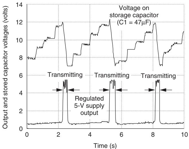
Figure 7 is a representative graph of signals from the power-conditioning circuitry with the PZT source during a walk. The upper trace shows the voltage across C1 (in this case, 47 µF), and the lower trace shows the MAX666 linear regulator’s output. Charge accumulates on the bucket capacitor, increasing with each step until the capacitor stores enough energy to power the transmitter for roughly half a second, generally after three to five steps with the current system. Substituting a high-frequency switching regulator for the MAX666 would further improve the efficiency of this circuit; this line of inquiry led to the results summarized in the following section.
line chart
| Time (s) | Output and stored capacitor voltages (volts) |
|---|---|
| 0 | 8 |
| 2 | 12 |
| 4 | 10 |
| 6 | 8 |
| 8 | 12 |
| 10 | 11 |
Figure 7. Stored voltage (top) and regulated power output (bottom) waveforms for shoe-powered RFID transmitter while walking.
Exploring high-frequency switching conversion
Despite its novelty, simplicity, and low quiescent power requirement, the shoe-powered RF tag system is inherently inefficient. Lowfrequency piezoelectric sources are essentially purely capacitive, and during walking they produce high-voltage, low-energy, low-dutycycle current pulses at approximately one cycle per second. This excitation profile results in an extremely high source impedance, with voltage signals in the hundreds of volts and currents on the order of 10-7 A. A linear regulation scheme, therefore, is not well suited to the electrical characteristics of a piezoelectric element excited by a brisk walk. For that reason, we devoted our subsequent research to finding a more efficient means of converting the raw electric energy produced by the transducers into a useful form. We explored various switching conversion schemes, including switched-capacitor converters and direct dc-dc down converters. In the end, we developed an offline, forward-switching converter, consisting of a small number of inexpensive, readily available components and materials.
A suitable low-frequency circuit model equivalent to a piezoelectric source consists of a capacitor in parallel with a resistor to model the dielectric leakage, and a charge source dependent on mechanical displacement to model the energy transduction. Because excitation occurs at such a low frequency and because the circuit should provide a stable, low-ripple output voltage, the power-conditioning system must perform low-pass filtering with an extremely low corner frequency. For that goal, the most efficient approach would be to discharge the source through a diode and a matched inductor into the bucket capacitor, ringing the circuit with each step. This technique is often used in ac charging circuits for capacitors in flash photography systems. At an average 1-Hz walking pace and a 140-nF source capacitance, however, resonant shunting requires an inductance on the order of 105 H. Certainly, such a value is not practical, especially if the device is to fit in a shoe.
Techniques for synchronously interrupting a resonant circuit have recently been proposed— for instance, allowing the ringing voltage on the source capacitance to swing up (or down) after the piezoelectric voltage has peaked (or reached a minimum).10 The resonant frequency is then made independent of the excitation period. Although this allows a resonance frequency much higher than the 1-Hz walk, any significant energy storage advantage could still require an impractically large inductor.
Switching converters are the natural alternative to resonant shunting because they offer two distinct advantages over linear systems. First, because they are truly power converters and not voltage regulators, switching converters are much more efficient when the difference between input and output voltages is large. Second, they function as impedance converters because the average dc output current can be larger than the average dc input current. Further, we selected the forward-converter topology because the step-down transformation shows a high reflected impedance to the piezoelectric source when the switch is closed. It also reduces switch stresses when the difference between input and output voltages is large and allows the simplest gate drive circuitry.
The piezoelectric power system presented here has much different characteristics and boundary conditions from those in normal switching-converter applications. Therefore, using commercially available control ICs was inappropriate, and much of the theory and practice common to switcher implementation didn’t apply. Specifically, the following points had particular weight in our converter topology selection and design:
• A low-frequency piezoelectric source is essentially a capacitor and a parallel charge source, and describes the energy stored on a capacitor. Therefore, it is advantageous to allow the source voltage to peak before removing the energy.
• The charge liberated per cycle is relatively constant under the same peak loading force, regardless of frequency.
Output ripple is dominated by the low excitation frequency of walking. Therefore, a large output capacitance (greater than 100 µF) is necessary to keep voltage ripple within acceptable limits.
text_image
D1 D4 R1 Rc1 Dp2 A+ V+ A- MAX934a B+ Bo V- REF GND C1 C2 Rr1 Rr2 D Vdd Q U2B Q ck S Vss Q̅ Ra Rb Ct Cvc V+ R ICM7555 OUT TH TR GND VC D Vdd Q U2A Q ck S Vss Q̅ T1 P Ms D5 L1 S Ds1 T D5 Ds2 L2 Cs R2 Q1 Zb R3 R4 Mg LGND … q(t) PZT dimorph source D3 D4 SGND
text_image
V+ R5 D+ V+ Do D- MAX934b C+ C- REF Co GND R’ U1B Q U1C S V_in SENSE LBO V_out MAX666 LBI SHDN V_set GND R6 V_out R7
LGND
Figure 8. Forward-switching converter system.
• Duty-cycle control is not an issue—we implemented switching simply to provide current gain.
• The average source current is very small (approximately 100 nA), so we selected semiconductor switches to minimize gate charge, not the drain-to-source On resistance.
We chose the switching frequency to minimize system energy loss, specifically in the transformer, switch control, and gate drive.
• The control circuitry must bootstrap itself from a cold startup; no battery is included to start the switching regulator.
Forward-switching converter design and operation
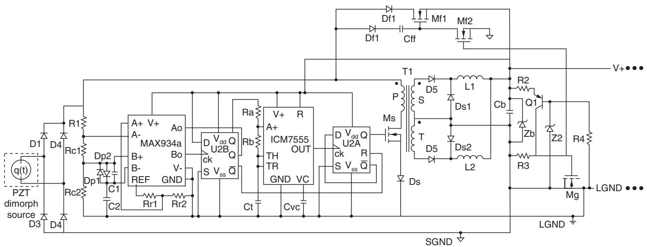
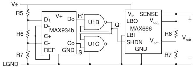
Figure 8 shows a block diagram of our forward-switching power-conditioning system. Note that this system has two ground buses— one referenced to the PZT source, the second to the load. We refer to these ground references as source ground (SGND) and load ground (LGND). Mg, an n-channel MOS-FET (metal-oxide semiconductor field-effect transistor), joins the two buses; Mg’s source connects to SGND and its drain to LGND. Because bucket capacitor Cb is sufficiently discharged and Z2 is not conducting at startup, resistor R3 pulls Mg’s gate to SGND. This configuration assures that SGND and LGND do not reference each other at startup and do not do so until Q1 goes into conduction. This latching circuit is identical to the one in Figure 6; we recycled it here for bootstrapping.
The source signal is full-wave rectified by a diode bridge (D1 to D4). Because LGND is not referenced to the source and Q1 is Off at startup, the only current path available to the rectified source signal is through the feed-forward loop and into Cb. Diodes Df1, D5, D6, Ds1, and Ds2 prevent Cb from discharging back through transformer T1 as it charges. To ensure Mf1 is On at startup, we placed Df2 and Cff in series on a second feed-forward branch to couple charge onto its gate. Further, Mf2’s gate shares the same node as Mg’s gate (that is, they share the same conduction state), so Mf2 is Off at startup and charge accumulates on Mf1, holding it On. Note that both Mf1 and Mf2 must be low-leakage, high-standoffvoltage devices. It is desirable to minimize source charge leakage through Mf1 after the switcher is operating, and a leaky Mf2 would strip charge off the Mf1 gate during startup.
As Cb charges beyond Z2’s breakdown voltage plus the diode drop across the Q1 baseemitter junction, Q1 is forced into conduction, which in turn activates Mf2 and Mg. With Mf2 On, Mf1’s gate is pulled to ground and current flow through the feed-forward loop is blocked in both directions. Most high-standoff-voltage MOSFETs have a body diode connected from source to drain, so we included Df1 to prevent reverse current flow through Mf1. Further, in the On state, Mg references LGND to SGND, which will then differ only by the voltage drop across the channel. Cb now has a current path through the conditioning circuitry and into the common ground, and the system is activated. LGND remains a viable current-return path until the voltage across R3 goes low enough to pinch off Mg. Adjusting the ratio between R2 and R3 can set the Cb voltage at which this occurs.
Once the control and regulation circuitry is activated and the direct current path from the source to the secondary side opens, the only means to transfer energy from the source into Cb is through the transformer and the MOS-FET switch. A peak detector (Dp1, Dp2, C1, and C2) and comparators A and B in the MAX934 IC perform zero-slope peak detection of the source signal. The switcher is activated when the signal reaches its maximum voltage and deactivated when a low signal is detected. Further, Ms is held open at startup so that the transformer will not load the source. R1, Rc1, and Rc2 constitute a very high resistance voltage divider (R1 is approximately 100 MΩ), and Rr1 and Rr2 divide the reference voltage (1.182 V) so that the input voltage at pin A− is limited as the source voltage approaches 300 V. Ao therefore remains High until the source signal voltage reaches the preset level and A− becomes greater than A+; the Reset pin on FF2 is then set Low. As the input signal continues to rise, the voltage drop across Dp2 holds B− higher than B+, thereby keeping Bo Low as C2 charges.
When the slope of the source signal reaches zero and begins to fall, the voltage across C2 is greater than the signal voltage, and the voltage drop across Dp1 causes the comparator to drive the Bo pin High. With Reset Low and a positive slope edge at the clock input of
U2B, the flip-flop latches Q high, thereby supplying power to the biasing circuitry of the ICM7555 CMOS oscillator. In using the Q pin to source this current, we reduce quiescent losses in the biasing resistors by supplying power only when the oscillator is needed. The oscillator will function as long as Q is High and the biasing circuitry is powered. It will remain High until the input signal falls below the threshold set at A+ and Reset is driven High. Further, feeding Ao into Reset prevents the oscillator from being turned On until the input signal reaches the A+ threshold, regardless of the source signal. This convention prevents small signals, such as the ones produced by weight shifts on the insole, from inadvertently activating the switcher. Rc1, Rc2, and C1 bias and filter the signal into the B−/B+ peak detector. We selected these values experimentally, and the circuit behaves somewhat erratically without them.
The forward-converter switcher conventionally operates at or near a 50 percent duty cycle to minimize switch stress and core losses (this regulator circuit8 achieves optimal performance at a 25-kHz switching frequency). However, biasing-circuitry losses approach a maximum as the duty cycle goes to 50 percent using the 7555 timer in this standard astable configuration. Simply, the Rb/Ra ratio should be made as small as practical to minimize losses, but it is impossible to reduce this ratio and approach a 50 percent duty cycle simultaneously. To address this quandary, we used a second D flip-flop to establish a perfect 50 percent duty-cycle square wave and drive the gate of the n-channel MOSFET switch Ms. We could then minimize the Rb/Ra ratio and use the 7555 to supply momentary trigger pulses to the flip-flop.
Therefore, at the peak of every current pulse from the dimorph source, the gate drive circuit switches an exponentially decaying source envelope through the step-down transformer T1 and into the storage stage. The T1 primary is coupled into two windings with the same turn ratio, N. S is the secondary winding, and tertiary winding T is inverted with respect to SGND. We use T to reset the magnetic flux through the transformer core during switch Off periods, transferring the magnetization energy into Cb.
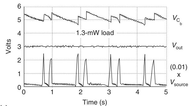
Following D5 and D6 are filter inductors and freewheeling diodes for both low-side windings. L1 (and L2 on the tertiary) and Cb form a second-order filter, normally implemented to reduce the high-frequency ripple at the output. In this design, the filter must contend with the source’s dominant 1-Hz excitation frequency. The inductors therefore operate discontinuously and do little to filter the dominant ripple. We included them merely to support the voltage difference between Cb and the transformed source when the switch is closed. The bucket capacitor is large enough to sustain an operable voltage between each current pulse (as shown in Figure 9a), and Zb protects the control circuitry if the voltage on Cb approaches the supply rating of the CMOS logic.
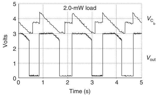
The final stage is for load switching. In this stage, two comparators and a NAND Set/Reset latch sense V+ and provide hysteresis in the LDO linear regulator’s On/Off control. This combination provides a regulated output voltage, prevents Cb from draining completely, and thereby reduces the number of slow bootstrapped restarts. Hysteresis is important because it prevents jitter or oscillation in load stage control and allows low-duty-cycle operation, as shown in Figure 9b, if a load demands higher power than the system provides.
Compared with the simple scheme of Figure 6, the switching converter proved a better means of conditioning power harvested from piezoelectric sources, although its efficiency was not as high as we anticipated. Figure 9a shows that the forward converter can supply at least 1.3 mW continuously at a walking pace of 0.8 Hz. Comparing this with the dimorph source’s raw power (8.4 mW at 1.1 Hz) and normalizing with respect to a common frequency, we found that the converter’s electrical efficiency is 17.6 percent. This result is better than twice the original linear regulator’s efficiency using the same source and bucket capacitor.7 More important, the switching-converter system provides electric power continuously during walking, a requirement of many potential applications.
Related work and future developments
Research is necessary in a few areas to enhance the efficiency and output of the two shoe-power-harvesting systems presented here. For better performance from the switching regulator, several electrical design factors need closer examination. The switching converter incurs losses in the transformer core and switching MOSFET. We could reduce these losses by using components tailored to micropower signals. Finally, applying soft-switching techniques and developing an optimal circuit layout would further reduce electrical system overhead.
line chart
| Time (s) | V_Cb (Volts) | V_out (Volts) | V_source (Volts) |
|---|---|---|---|
| 0 | ~5.5 | ~3.0 | ~0.0 |
| 1 | ~5.5 | ~3.0 | ~2.5 |
| 2 | ~5.5 | ~3.0 | ~2.5 |
| 3 | ~5.5 | ~3.0 | ~2.5 |
| 4 | ~5.5 | ~3.0 | ~2.5 |
| 5 | ~5.5 | ~3.0 | ~2.5 |
(a)
line chart
| Time (s) | V_Cb (Volts) | V_out (Volts) |
|---|---|---|
| 0 | 3.8 | 3.0 |
| 1 | 4.5 | 0.0 |
| 2 | 3.8 | 3.0 |
| 3 | 3.0 | 0.0 |
| 4 | 3.8 | 3.0 |
| 5 | 3.8 | 3.0 |
(b)
Figure 9. Switching converter signals for a continuous 1.3-mW load (a) and a 2.0-mW load (b), showing low-voltage shutdown. Both examples resulted from walking with the PZT dimorph source, represented in the bottom plot of (a).
Without straying from the relative simplicity of low-frequency passive excitation, the logical next steps for the piezoelectric shoe power system are refining the transformer and FET switch designs and developing an integrated circuit to perform control. Commercially available high-voltage FETs are built for high-current applications. They have relatively high gate charge requirements, and the gate drive dissipates a large portion of a piezoelectric source’s power even at low frequencies. The most important enhancement therefore is to optimize the switching transistor for high voltages but very small currents. Further, placing the control on an IC would reduce losses associated with coupling multiple discrete components and force the development of an optimal layout. Layout is often just as important as component selection to the performance of a switching converter. A better layout could reduce switching noise and eliminate stray resonances that degrade the discrete design’s performance.
natural_image
Close-up of a mechanical device with internal components and a black tab, no visible text or symbols
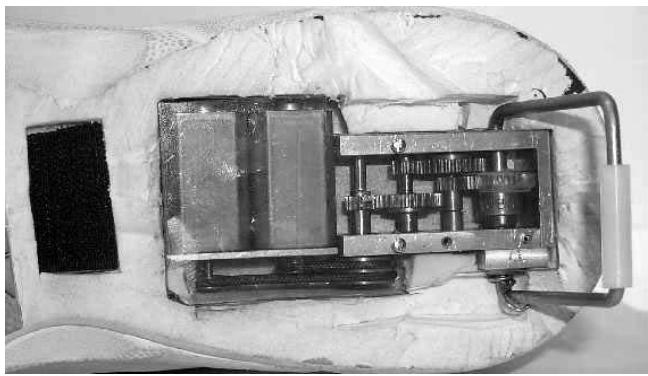
Figure 10. Pair of rotary magnetic generators embedded in a sneaker sole with step-up gear mechanisms.
Of prime importance in obtaining better performance is improving the mechanics of exciting the transducer from foot dynamics. An aspect not fully addressed here is the physical impedance match between foot and transducer. We selected the piezoelectric elements’ dimensions and mechanical braces to balance comfort and energy transfer, but a more rigorous study, depending on specific applications, is needed. Also, piezoelectric elements have been used for many years to actively damp the high-frequency mechanical vibrations. We could apply those relationships in reverse by artificially exciting the material near its mechanical resonance and against the force of the downward footstep, liberating a larger net electrical energy.
Cyclic mechanical excitation near the material’s resonant frequency can make a piezoelectric element undergo many efficient charge/discharge cycles during a single heel strike. As a result, the element would produce much more energy, potentially extracting a few watts of power from a heel strike.11 This scheme is mechanically more complicated than the simple insole mounting schemes shown earlier in Figure 2, making the piezoelectric generators too large to be easily embedded.
Developers in the United Kingdom have reported on recent experiments using a boot with inserted piezoelectric crystals,12 and approaches of this sort have been explored for mobile medical applications.4 The power output of these devices is said to be more than an order of magnitude beyond the levels presented in this article. But conventional piezoelectric crystals and ceramics are much stiffer than the materials used in our generators, potentially requiring a hard-hit excitation through a mechanical linkage or indirect excitation through modulated hydraulics.4,11 These techniques would possibly impact the look and feel of the shoe, as well as the generator’s longevity and mechanical complexity.
Other proposed designs use electroactive polymers to achieve a similar level of power, with the generator (a rubbery dielectric material) mounted in the compressible heel of the shoe.13 These designs require a very high potential (such as several kilovolts) to be applied across the dielectric (because current is produced as the material is compressed and its capacitance changes). Hence, achieving efficient power conditioning is challenging in these systems.
Moving-magnet systems likewise involve a more complicated integration,14 but they can become competitive because of their high efficiency and well-established technology. As an example, we conducted a simple test of a foot-mounted rotary generator.7 Our device significantly hampered the wearer’s gait because of its primitive mechanical linkage. However, it generated an average of 250 mW, two orders of magnitude higher than the results from the piezoelectric systems presented here.
We further explored integrating the magnetic generators and their associated mechanics into the shoe sole itself.15 Figure 10 shows an example that generated approximately 60 mW of average power. Adding mechanical energy storage, such as a clock spring, would allow more energy to be harvested per footfall (driving the generator continuously between steps), increasing the resulting power to about one watt. Their abundant moving parts, high gear ratios, and intrinsic complexity, however, can make these devices fragile and expensive. Better engineering—for example, driving a magnetic generator via a hydraulic link to reservoirs compressing with the sole16—can produce a longer-lived device that generates considerably more power than our piezoelectric sources.
fter improving the shoe-generator useful body-worn systems. The RFID transmitter is one example of a simple and practical application of scavenged shoe power. However, at such low power levels, embedded batteries might be a viable (but environmentally unfriendly) alternative, depending on the frequency of use and product lifetime. Other possibilities include a personal positioning system for military or police units, a personal navigator or smart pedometer, a data collection tool for monitoring an athlete’s movements, and a child-tracking device. There are countless other potential applications.
As the power yield increases and wearable electronics become more efficient, foot-powered energy-harvesting systems can drive more components of wearable computers, eliminating the need for batteries or enabling them to be charged “on the hoof.” These systems would open a host of applications in situations where power grid access is often unavailable, such as extended hiking expeditions or military missions.
As applications increase, so should ease of use. The piezoelectric insole and conditioning electronics could be marketed as separate components to be modularly linked to electronics embedded in the heel via a weatherproof connector. As insoles wore out, consumers would replace or upgrade them. With appropriate adaptations, shoe-mounted energy-scavenging systems are likely to power a wide range of body-worn devices. MICRO
Acknowledgments
We are grateful to our MIT Media Lab collaborators Jake Kendall, John Kymissis, and Neil Gershenfeld of the Physics and Media Group. We also thank our associates in the Media Lab’s sponsor community, in particular Kyung Park and Minoru Toda at the Sensor Products Division of Measurement Specialties (formerly AMP Sensors) for working with us on the design of the PVDF stave and providing the foil. We acknowledge helpful and interesting discussions with many other research colleagues, especially Robert Nowak of the Defense Advanced Research Projects Agency and Nesbit Hagood of MIT. We appreciate the support of the Things That Think Consortium and our other sponsors at the MIT Media Laboratory.
Nathan Shenck is grateful to the C.S. Draper Laboratory in Cambridge, Mass., for the opportunity to study at MIT as a Draper Fellow while conducting research at CSDL and the MIT Media Lab. He acknowledges the US Navy for granting him a two-year leave of service to pursue graduate education. He also thanks John Sweeney, Richard Gardener, and Paul Rosenstrach for guidance and support at CSDL.
References
- T. Starner, “Human Powered Wearable Computing,” IBM Systems J., vol. 35, nos. 3 and 4, 1996, pp. 618-629.
- J.P. Marsden and S.R. Montgomery, “Plantar Power for Arm Prosthesis Using Body Weight Transfer,” Human Locomotor Engineering, Inst. Mechanical Engineers Press, London, 1971, pp. 277-282.
- R. Fletcher, “Force Transduction Materials for Human-Technology Interface,” IBM Systems J., vol. 35, nos. 3 and 4, 1996, pp. 630-638.
- J.F. Antaki et al., “A Gait Powered Autologous Battery Charging System for Artificial Organs,” Proc. 1995 American Society of Artificial Internal Organs Conf., Lippincott Williams & Wilkins, Philadelphia, 1995, pp. M588-M595.
- “Piezoelectric Tutorial,” Piezo Systems, Cambridge, Mass.; http://www.piezo.com/ intro.html.
- C.J. Kendall, Parasitic Power Collection in Shoe-Mounted Devices, BS thesis, Dept. of Physics and MIT Media Laboratory, Massachusetts Institute of Technology, Cambridge, Mass., June 1998.
- J. Kymissis et al., “Parasitic Power Harvesting in Shoes,” Second IEEE Int’l Conf. Wearable Computing, IEEE CS Press, Los Alamitos, Calif., 1998, pp. 132-139.
- N. Shenck, A Demonstration of Useful Electric Energy Generation from Piezoceramics in a Shoe, MS thesis, Dept. of Electrical Engineering and Computer Science, Massachusetts Institute of Technology, Cambridge, Mass., 1999.
- R. Want et al., “The Active Badge Location System,” ACM Trans. Information Systems, vol. 10, no. 1, Jan. 1992, pp. 91-102.
- P. Smalser, Power Transfer of Piezoelectric Generated Energy, US patent 5703474, Patent and Trademark Office, Washington, D.C., 1997.

text_image
Next- generation courses for the next generation of computer professionals Influence what our students learn. Review the latest draft of Computing Curricula 2001. http://computer.org/education/curricula2001 Prepared by the IEEE Computer Society/ACM joint task force on Computing Curricula 2001 IEEE COMPUTER SOCIETY acm
- N. Hagood et al., “Development of Micro-Hydraulic Transducer Technology,” Proc. 10th Int’l Conf. Adaptive Structures and Technologies, Technomic Publishing, Lancaster, Penn., 1999, pp. 71-81.
- J. Drake, “The Greatest Shoe on Earth,” Wired, vol. 9, no. 2, Feb. 2001, pp. 90-100.
- R.E. Pelrine, R.D. Kornbluh, and J.P. Joseph, “Electrostriction of Polymer Dielectrics with Compliant Electrodes as a Means of Actuation,” Sensors and Actuators A: Physical, vol. 64, no. 1, 1998, pp.77-85.
- N. Lakic, Inflatable Boot Liner with Electrical Generator and Heater, US patent 4845338, Patent and Trademark Office, Washington, D.C., 1989.
- J. Hayashida, Unobtrusive Integration of Magnetic Generator Systems into Common Footwear, BS thesis, Dept. of Electrical Engineering and MIT Media Laboratory, Massachusetts Institute of Technology, Cambridge, Mass., 2000.
- E. Tkaczyk, “Technology Summary,” Prospector IX: Human-Powered Systems Technologies, M.F. Rose, ed., Space Power Institute, Auburn Univ., Auburn, Ala., 1997, pp. 38-43.
Nathan S. Shenck is a submarine lieutenant on the USS Philadelphia, stationed in Groton, Connecticut. While not at sea, he enjoys investigating alternative energy sources and researching wireless technology. Shenck has a BS in electrical engineering from the US Naval Academy and an MS in electrical engineering from MIT.
Joseph A. Paradiso is a principal research scientist at the MIT Media Laboratory, where he leads the Responsive Environments Group and is the Technology Director of the Things That Think Consortium. In earlier work, he developed high-energy physics detectors, spacecraft control algorithms, and various sensor systems. Paradiso has a BS in electrical engineering and physics from Tufts University and a PhD in physics from MIT, where he was a Compton Fellow. He is a member of the IEEE, AIAA, ACM, and APS.
Direct questions and comments about this article to Joseph A. Paradiso, Responsive Environments Group, MIT Media Laboratory, Cambridge, MA 02139; joep@media.mit.edu.